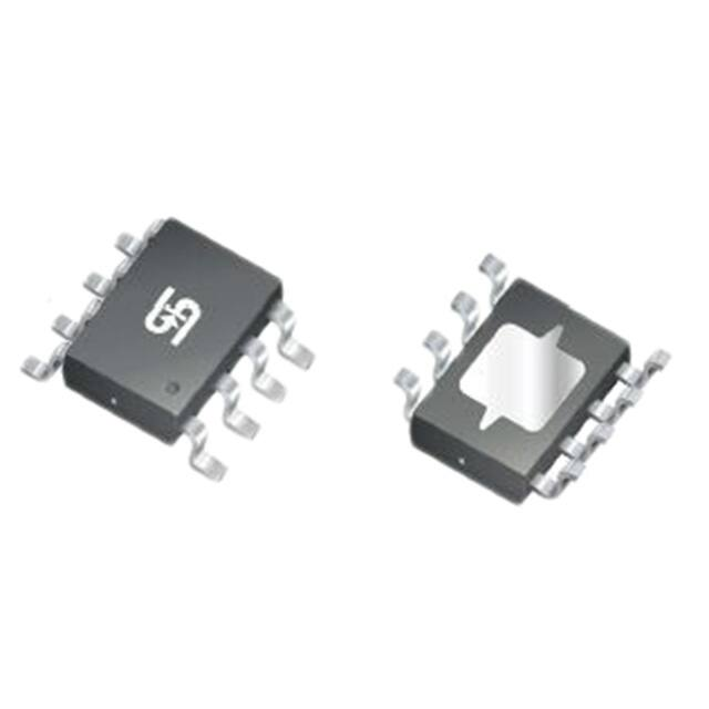
TS103ACS
Taiwan Semiconductor
Dual Operational Amplifiers and Voltage Reference
DESCRIPTION
FEATURES
The TS103 is a monolithic IC specifically designed to
●
Input Offset Voltage: 0.5mV
control the output current and voltage levels of switch
●
Supply Current: 250μA per OP AMP @ 5V
mode battery chargers and power supplies. The device
●
Unity Gain Bandwidth: 1MHz
contains two operational amplifiers and a precision
●
Output Voltage Swing: 0~(VCC – 1.5) V
shunt regulator. OP AMP 1 is designed for voltage
●
Power Supply Voltage: 3~18V
control, whose non-inverting input internally connects to
●
Fixed Output Voltage Reference: 2.5V1%
the output of the shunt regulator. OP AMP 2 is for
●
Sink Current Capability from 0.2~80mA
current control with both inputs uncommitted. The IC
●
RoHS Compliant
offers the power converter designer a control solution
●
Halogen-free according to IEC 61249-2-21
that features increased precision with a corresponding
APPLICATION
reduction in system complexity and cost.
SOP-8
●
Battery chargers
●
Switch-Mode Power Supplies
●
Linear voltage regulation
Pin Definition:
1. Output A
2. Input A (-)
3. Input A (+) / VKA
4. GND
8. VCC
7. Output B
6. Input B (-)
5. Input B (+)
Note: MSL 3 (Moisture Sensitivity Level) per J-STD-020
TYPICAL APPLICATION CIRCUIT
1
Version: E2103
�TS103ACS
Taiwan Semiconductor
ABSOLUTE MAXIMUM RATINGS (Note 1)
PARAMETER
SYMBOL
LIMIT
UNIT
VCC
20
V
VIN
-0.3 to VCC +0.3
V
VID
20
V
IK
100
mA
PD
500
mW
TSTG
-65 to 150
°C
--
≥200
V
PARAMETER
SYMBOL
CONDITIONS
UNIT
Supply Voltage
VCC
3 ~ 18
V
Operating Ambient Temperature Range
TOPA
-40 to +85
°C
Power Supply Voltage (VCC to GND)
Op Amp 1 and 2 Input Voltage Range
Op Amp 2 Input Differential Voltage
Voltage Reference Cathode Current
(Pins 2,5,6)
(Pins 5,6)
(Pin 3)
Power Dissipation
Storage Temperature Range
ESD Protection Voltage (Machine Model)
RECOMMENDED OPERATING CONDITIONS
(Note 3)
ELECTRICAL SPECIFICATIONS (VCC = 18V, TA = 25°C unless otherwise noted)
PARAMETER
CONDITIONS
MIN
TYP
MAX
--
0.5
0.8
VCC= 5V, no load,
Total Supply Current, excluding
Current in Voltage Reference
-40°C ≤ TA ≤ 85°C
UNIT
mA
VCC= 18V, no load,
--
0.6
1.2
IKA = 10mA
2.490
2.500
2.510
IKA = 10mA @ -40°C ≤ TA ≤ 85°C
2.475
2.500
2.525
IKA = 10mA,
--
TA= -40 to 85°C
--
5
5
24
17
mV
--
0.2
1.0
mA
0.3
0.5
Ω
--
0.5
2
TA = -40 to 85°C
--
--
5
Input Offset Voltage
Temperature Drift
TA = -40 to 85°C
--
7
--
µV/°C
Input Bias Current
(Inverting Input Only)
TA = 25°C
--
20
150
nA
85
100
--
dB
-40°C ≤ TA ≤ 85°C
Voltage Reference Section
Reference Voltage
Reference Voltage Deviation
Over Full Temperature Range
Minimum Cathode Current
for Regulation
Dynamic Impedance
VCC = 1~80mA, f
很抱歉,暂时无法提供与“TS103CS RLG”相匹配的价格&库存,您可以联系我们找货
免费人工找货- 国内价格 香港价格
- 5000+1.742065000+0.22629