NJU7076/NJU7077/NJU7078
PRECISION, LOW NOISE, RAIL-TO-RAIL OUTPUT,
EXCELLENT EMI IMMUNITY, CMOS OPERATIONAL AMPLIFIERS
FEATURES
DESCRIPTION
●High Precision
Low Input Offset Voltage
NJU7076 / NJU7077
150μV max.
NJU7078
200μV max.
Low Offset Voltage Drift
0.5μV/°C typ.
●Low Noise
10nV/√Hz typ.
●Low Input Bias Current
1pA typ.
●Rail-to-Rail Output
RL=10kΩ
0.02V to 4.98V typ. (V+=5V)
RL=600Ω
0.08V to 4.92V typ. (V+=5V)
●Ground Sensing
●Integrated EMI Filter EMIRR=59dB typ. @f=900 MHz
●Operating Voltage
2.2V to 5.5V
●Unity-Gain Stable
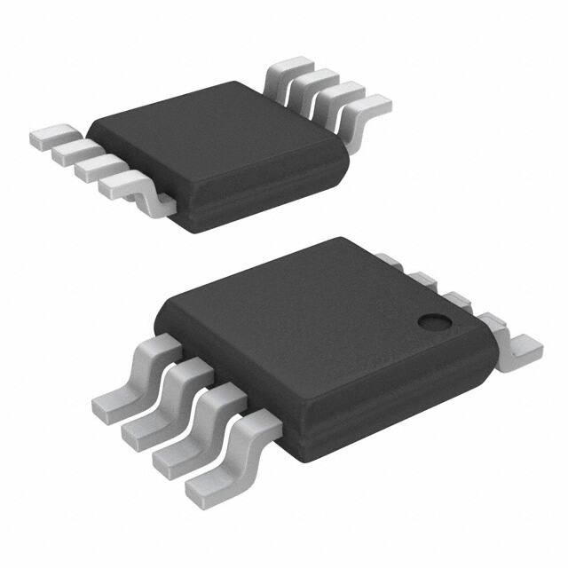
●Package
NJU7076
SOT-23-5
NJU7077
MSOP8 (VSP8)*
The NJU7076/NJU7077/NJU7078 are single/dual/Quad
channel, precision, low-noise, rail-to-rail output CMOS
operational amplifiers. These devices featuring a low input
offset voltage (50µV max.), low temperature drift (0.5µV/°C
typ.), and low bias current (1pA typ.). The combination of
these specifications makes the devices well-suited for sensor
applications such as temperature sensors, weight sensors,
high-precision current sensing amplifiers, and current-voltage
converters.
The output swing can reach 20 mV from the rails while driving
a 10kΩ load (at 5V operation). Input voltage includes ground,
enabling direct sensing near ground.
The NJU7076/NJU7077/NJU7078 have high EMI immunity
to reduce malfunctions, making them ideal for EMI-sensitive
applications.
*meet JEDEC MO-187-DA
NJU7078
SSOP14
APPLICATIONS
●Thermocouple / Thermopile Amplifiers
●Strain Gauge / Pressure Sensor Amplifiers
●Load Cell and Bridge Transducer Amplifiers
●High-Resolution Data Acquisition
●Precision Current Sensing
●Battery Monitoring
●Photodiode Amplifiers
■ TYPICAL CHARACTERISTICS
Voltage Noise Density vs. Frequency
Input Offset Voltage vs. Temperature
V+=5V, V-=0V, VCOM =V+/2
Equivalent Input Noise Voltage [nV/√Hz]
500
Input Offset Voltage [μV]
400
300
200
100
0
-100
-200
-300
-400
-500
-50
Ver.6.2
-25
V+=5V, V-=0V, Ta=25ºC
100
90
80
70
60
50
40
30
20
10
0
0
25 50 75 100 125 150
Ambient Temperature [ºC]
www.njr.com
1
10
100
Frequency [Hz]
1k
10k
-1-
�NJU7076/NJU7077/NJU7078
■ PIN CONFIGURATIONS
PRODUCT NAME
NJU7076F
NJU7077R
Package
SOT-23-5
MSOP8 (VSP8)
(Top View)
(Top View)
OUTPUT
1
V-
2
+INPUT
3
Pin Functions
5
4
A OUTPUT
1
8
V+
A -INPUT
2
7
B OUTPUT
A +INPUT
3
6
B -INPUT
V-
4
5
B +INPUT
V+
-INPUT
PRODUCT NAME
NJU7078V
Package
SSOP14
(Top View)
Pin Functions
A OUTPUT
1
14
D OUTPUT
A -INPUT
2
13
D -INPUT
A +INPUT
3
12
D +INPUT
V+
4
11
V-
B +INPUT
5
10
C +INPUT
B -INPUT
6
9
C -INPUT
B OUTPUT
7
8
C OUTPUT
■ PRODUCT NAME INFORMATION
NJU7076
Part Number
F
(TE1)
Package
Taping Form
■ ORDER INFORMATION
PRODUCT
NAME
PACKAGE
RoHS
HALOGENFREE
TERMINAL
FINISH
MARKING
WEIGHT
(mg)
MOQ
(pcs)
NJU7076F
SOT-23-5
Yes
Yes
Sn2Bi
11D
15
3000
NJU7077R
MSOP8 (VSP8)
Yes
Yes
Sn2Bi
7077
21
2000
NJU7078V
SSOP14
Yes
Yes
Sn2Bi
7078
65
2000
Ver.6.2
www.njr.com
-2-
�NJU7076/NJU7077/NJU7078
■ ABSOLUTE MAXIMUM RATINGS
PARAMETER
SYMBOL
+
Supply Voltage
V -V
Differential Input Voltage
(1)
-
VID
Input Voltage
RATING
UNIT
7
V
±7
(2)
-
VIN
V
(3)
V -0.3 to V⁺+0.3
Power Dissipation (Ta=25°C)
SOT-23-5
MSOP8 (VSP8)
SSOP14
Storage Temperature Range
Tstg
2-Layer / 4-Layer(4)
480 / 650
500 / 660
555 / 690
-55 to 150
Maximum Junction Temperature
Tjmax
150
SYMBOL
VALUE
PD
V
mW
°C
°C
■ THERMAL CHARACTERISTICS
PACKAGE
Junction-to-Ambient Thermal Resistance
SOT-23-5
MSOP8 (VSP8)
SSOP14
Junction-to-Top of Package Characterization Parameter
(1)
(2)
(3)
(4)
UNIT
(4)
2-Layer / 4-Layer
260 / 192
250 / 189
225 / 181
2-Layer / 4-Layer(4)
Θja
ºC/W
SOT-23-5
67 / 58
Ψjt
ºC/W
MSOP8 (VSP8)
62 / 53
SSOP14
53 / 52
Differential voltage is the voltage difference between +INPUT and -INPUT.
For supply voltage less than 7V, the absolute maximum rating is equal to the supply voltage.
The absolute maximum input voltage is limited at 7V.
2-Layer: Mounted on glass epoxy board. (76.2×114.3×1.6 mm: based on EIA/JDEC standard, 2-layer FR-4)
4-Layer: Mounted on glass epoxy board. (76.2×114.3×1.6 mm: based on EIA/JDEC standard, 4-layer FR-4), internal Cu
area: 74.2 x 74.2 mm
■ POWER DISSIPATION vs. AMBIENT TEMPERATURE
Power Dissipation vs. Temperature
Power Dissipation vs. Temperature
4-Layer
800
800
700
700
Power Dissipation PD [mW]
Power Dissipation PD [mW]
2-Layer
SSOP14
600
500
400
MSOP8 (VSP8)
300
200
SOT-23-5
100
0
SSOP14
600
MSOP8 (VSP8)
500
400
300
SOT-23-5
200
100
0
0
25
50
75
100 125
Ambient Temperature [°C]
150
0
25
50
75
100 125
Ambient Temperature [°C]
150
■ RECOMMENDED OPERATING CONDITIONS
PARAMETER
Supply Voltage
Operating Temperature Range
Ver.6.2
SYMBOL
+
V -V
-
CONDITIONS
Ta=25˚C
Topr
www.njr.com
VALUE
UNIT
2.2 to 5.5
V
-40 to 125
°C
-3-
�NJU7076/NJU7077/NJU7078
■ ELECTRICAL CHARACTERISTICS (V+=5V, V-=0V, VCOM=V+/2, Ta=25˚C, unless otherwise noted.)
PARAMETER
SYMBOL
TEST CONDITIONS
MIN
TYP
MAX
UNIT
100
20
20
0.5
1
1
130
150
400
200
400
5
-
100
-
-
70
70
70
70
4.95
4.95
4.85
4.85
4.9
4.85
0
0
90
90
4.98
4.92
4.96
0.02
0.08
0.04
-
0.05
0.05
0.15
0.2
0.1
0.15
4
4
-
0.6
1.2
2.3
-
0.9
0.9
1.8
1.8
3.5
3.5
-
1.3
-
MHz
-
60
-
deg
-
12
-
dB
-
10
-
nV/√Hz
-
0.5
-
V/µs
-
0.01
-
%
-
140
-
dB
DC CHARACTERISTICS
Input Offset Voltage
NJU7076 / NJU7077
VIO
Ta=-40°C to 125°C
NJU7078
Input Offset Voltage Drift
Input Bias Current
Input Offset Current
ΔVIO/ΔT
IB
IIO
Open-Loop Voltage Gain
AV
Common-Mode Rejection Ratio
CMR
Supply Voltage Rejection Ratio
SVR
High-level Output Voltage
VOH
Low-level Output Voltage
VOL
Common-Mode Input Voltage Range
VICM
Supply Current (All Amplifiers)
NJU7076
NJU7077
ISUPPLY
NJU7078
Ta=-40°C to 125°C
Ta=-40°C to 125°C (5)
Vo=0.5V to 4.5V, RL=10kΩ to 2.5V
Vo=0.5V to 4.5V, RL=10kΩ to 2.5V,
Ta= -40°C to 125°C
VICM=0V to 4V
VICM=0V to 4V, Ta= -40°C to 125°C
V+=2.2V to 5.5V
V+=2.2V to 5.5V, Ta= -40°C to 125°C
RL=10kΩ to 2.5V
RL=10kΩ to 2.5V, Ta= -40°C to 125°C
RL=600Ω to 2.5V
RL=600Ω to 2.5V, Ta= -40°C to 125°C
ISOURCE=2mA
ISOURCE =2mA, Ta= -40°C to 125°C
RL=10kΩ to 2.5V
RL=10kΩ to 2.5V, Ta= -40°C to 125°C
RL=600Ω to 2.5V
RL=600Ω to 2.5V, Ta= -40°C to 125°C
ISINK=2mA
ISINK=2mA, Ta= -40°C to 125°C
CMR≥70dB
CMR≥70dB, Ta= -40°C to 125°C
No Signal
No Signal, Ta = -40°C to 125°C
No Signal
No Signal, Ta = -40°C to 125°C
No Signal
No Signal, Ta = -40°C to 125°C
µV
µV/°C
pA
pA
dB
dB
dB
V
V
V
mA
AC CHARACTERISTICS
GV=40dB, RF=100kΩ, RL=10kΩ to 2.5V,
CL=20pF, f=100kHz
GV=40dB, RF=100kΩ, RL=10kΩ to 2.5V,
Phase Margin
Φm
CL=20pF
GV=40dB, RF=100kΩ, RL=10kΩ to 2.5V,
Gain Margin
Gm
CL=20pF
Equivalent Input Noise Voltage
en
f=1kHz
GV=0dB, RL=10kΩ to 2.5V, CL=20pF,
Slew Rate
SR
VIN=3VPP
GV=20dB, RL=10kΩ to 2.5V, f=1kHz,
Total Harmonic Distortion + Noise
THD+N
VO=3VPP
Channel Separation
CS
f=1kHz, NJU7077 / NJU7078
(5) Guaranteed by two points of Temperature -40˚C and 125˚C
Gain Bandwidth Product
Ver.6.2
GBW
www.njr.com
-4-
�NJU7076/NJU7077/NJU7078
■ ELECTRICAL CHARACTERISTICS (V+=2.2V, V-=0V, VCOM=V+/2, Ta=25˚C, unless otherwise noted.)
PARAMETER
SYMBOL
TEST CONDITIONS
MIN
TYP
MAX
UNIT
100
60
60
0.6
1
1
130
250
400
300
400
5
-
100
-
-
70
70
2.15
2.15
2.1
2.05
2.05
2
0
0
90
2.18
2.14
2.13
0.02
0.06
0.07
-
0.05
0.05
0.1
0.15
0.15
0.2
1.2
1.2
-
0.55
1.0
2.0
-
0.82
0.82
1.5
1.5
3.0
3.0
-
1.2
-
MHz
-
60
-
deg
-
12
-
dB
-
10
-
nV/√Hz
-
0.5
-
V/µs
-
0.01
-
%
-
140
-
dB
DC CHARACTERISTICS
Input Offset Voltage
NJU7076 / NJU7077
VIO
Ta= -40°C to 125°C
NJU7078
Input Offset Voltage Drift
Input Bias Current
Input Offset Current
ΔVIO/ΔT
IB
IIO
Open-Loop Voltage Gain
AV
Common-Mode Rejection Ratio
CMR
High-level Output Voltage
VOH
Low-level Output Voltage
VOL
Common-Mode Input Voltage
Range
VICM
Supply Current (All Amplifiers)
NJU7076
NJU7077
ISUPPLY
NJU7078
Ta= -40°C to 125°C
Ta= -40°C to 125°C (5)
Vo=0.6V to 1.6V, RL=10kΩ to 1.1V
Vo=0.6V to 1.6V, RL=10kΩ to 1.1V,
Ta= -40°C to 125°C
VICM=0V to 1.2V
VICM=0V to 1.2V, Ta= -40°C to 125°C
RL=10kΩ to 1.1V
RL=10kΩ to 1.1V, Ta= -40°C to 125°C
RL=600Ω to 1.1V
RL=600Ω to 1.1V, Ta= -40°C to 125°C
ISOURCE=2mA
ISOURCE=2mA, Ta= -40°C to 125°C
RL=10kΩ to 1.1V
RL=10kΩ to 1.1V, Ta= -40°C to 125°C
RL=600Ω to 1.1V
RL=600Ω to 1.1V, Ta= -40°C to 125°C
ISINK=2mA
ISINK=2mA, Ta= -40°C to 125°C
CMR≥70dB
CMR≥70dB, Ta= -40°C to 125°C
No Signal
No Signal, Ta = -40°C to 125°C
No Signal
No Signal, Ta = -40°C to 125°C
No Signal
No Signal, Ta = -40°C to 125°C
µV
µV/°C
pA
pA
dB
dB
V
V
V
mA
AC CHARACTERISTICS
GV=40dB, RF=100kΩ, RL=10kΩ to 1.1V,
CL=20pF, f=100kHz
GV=40dB, RF=100kΩ, RL=10kΩ to 1.1V,
Phase Margin
Φm
CL=20pF
GV=40dB, RF=100kΩ, RL=10kΩ to 1.1V,
Gain Margin
Gm
CL=20pF
Equivalent Input Noise Voltage
en
f=1kHz
GV=0dB, RL=10kΩ to 1.1V, CL=20pF,
Slew Rate
SR
VIN=1VPP
GV=20dB, RL=10kΩ to 1.1V, f=1kHz,
Total Harmonic Distortion + Noise
THD+N
VO=1VPP
Channel Separation
CS
f=1kHz, NJU7077 / NJU7078
(5) Guaranteed by two points of Temperature -40˚C and 125˚C
Gain Bandwidth Product
Ver.6.2
GBW
www.njr.com
-5-
�NJU7076/NJU7077/NJU7078
■ TYPICAL CHARACTERISTICS
Input Offset Voltage vs. Temperature
V+=2.2V, V-=0V, VCOM =V+/2
500
400
400
300
300
Input Offset Voltage [μV]
Input Offset Voltage [μV]
Input Offset Voltage vs. Temperature
V+=5V, V-=0V, VCOM =V+/2
500
200
100
0
-100
-200
-300
-400
200
100
0
-100
-200
-300
-400
-500
-500
-50
-25
0
25 50 75 100 125 150
Ambient Temperature [ºC]
-50
-25
Input Offset Voltage Distribution
Input Offset Voltage Distribution
V+=5V, V-=0V, VCOM=V+/2, Ta=25ºC
40%
Number of Amplifiers [%]
Number of Amplifiers [%]
35%
30%
25%
20%
15%
10%
5%
30%
25%
20%
15%
10%
5%
0%
0%
-200
-100
0
100
Input Offset Voltage [μV]
200
-200
Input Offset Voltage Drift Distribution
-100
0
100
Input Offset Voltage [μV]
200
Input Offset Voltage Drift Distribution
V+=5V, V-=0V, VCOM=V+/2
40%
V+=2.2V, V-=0V, VCOM=V+/2
40%
35%
Number of Amplifiers [%]
35%
Number of Amplifiers [%]
V+=2.2V, V-=0V, VCOM=V+/2, Ta=25ºC
40%
35%
30%
25%
20%
15%
10%
5%
30%
25%
20%
15%
10%
5%
0%
0%
-2.5
Ver.6.2
0
25 50 75 100 125 150
Ambient Temperature [ºC]
-1.5 -0.5
0.5
1.5
2.5
Input Offset Voltage Drift [μV/ºC]
3.5
-2.5
www.njr.com
-1.5 -0.5
0.5
1.5
2.5
Input Offset Voltage Drift [μV/ºC]
3.5
-6-
�NJU7076/NJU7077/NJU7078
■ TYPIC AL CHARACTERISTICS
Input Offset Voltage
vs. Common-Mode Input Voltage
Input Offset Voltage vs. Supply Voltage
V+=5V, V-=0V
V-=0V, VCOM=V+/2
0.5
0.5
0.4
Input Offset Voltage [mV]
Input Offset Voltage [mV]
0.4
0.3
0.2
Ta=125ºC
Ta=25ºC
0.1
0
-0.1
-0.2
Ta=-40ºC
-0.3
-0.4
0.2
Ta=25ºC
0
-0.1
-0.2
Ta=-40ºC
-0.3
-0.5
0
1
2
3
4
5
Supply Voltage V+ [V]
6
7
-1
Warm-Up Vio Drift
V+=2.2V, V-=0V
V+=3.3V, V-=0V, VCOM=V+/2, Ta=25ºC
20
Input Offset Voltage Change [μV」
0.4
0.3
0.2
Ta=125ºC
0.1
Ta=25ºC
0
-0.1
-0.2
Ta=-40ºC
-0.3
-0.4
5
15
10
5
0
-5
-10
-15
-20
-0.5
-1
-0.5
0
0.5
1
1.5
Common-Mode Input Voltage [V]
0
2
Input Bias Current vs. Temperature
Open-Loop Voltage Gain [dB]
1500
1250
1000
V+=5V
500
20
30
40
Time [sec]
50
60
V-=0V, RL=10kΩ
160
1750
750
10
Open-Loop Voltage Gain vs. Temperature
V-=0V, VCOM=V+/2
2000
Input Bias Current [pA]
0
1
2
3
4
Common-Mode Input Voltage [V]
Input Offset Voltage
vs. Common-Mode Input Voltage
0.5
V+=2.2V
250
0
150
V+=5.0V
140
130
120
V+=2.2V
110
100
90
80
25
Ver.6.2
Ta=125ºC
0.1
-0.4
-0.5
Input Offset Voltage [mV]
0.3
50
75
100
125
Ambient Temperature [ºC]
150
-50
www.njr.com
-25
0
25 50 75 100 125 150
Ambient Temperature [ºC]
-7-
�NJU7076/NJU7077/NJU7078
■ TYPICAL CHARACTERISTICS
CMR vs. Frequency
V+=5V, V-=0V, VIN=1Vpp, RS=100Ω, RF=10kΩ, Ta=25ºC
120
Supply Voltage Rejection Ratio [dB]
Common-Mode Rejection Ratio [dB]
SVR vs. Frequency
V+=5V, V-=0V, VIN=1Vpp, RS=100Ω, RF=10kΩ, Ta=25ºC
120
110
100
90
80
70
60
100
+SVR
80
60
-SVR
40
20
10
100
1k
10k
Frequency [Hz]
100k
10
100
1k
10k
Frequency [Hz]
100k
Supply Current per Amplifier vs. Supply Voltage
GV=0dB
Supply Current per Amplifier [mA]
0.9
0.8
0.7
Ta=25°C
0.6
0.5
Ta=125°C
0.4
Ta=-40°C
0.3
0.2
0.1
0
0
1
2
3
4
5
Supply Voltage V+ [V]
6
7
Maximum Output Voltage vs. Output Current
Maximum Output Voltage vs. Output Current
V+=2.2V, V-=0V
V+=5V, V-=0V
2.2
5.0
4.5
Output Voltage [V]
Ta=25ºC
3.5
Ta=-40ºC
3.0
2.5
2.0
Ta=-40ºC
1.5
Ta=25ºC
1.0
Ta=25ºC
1.4
1.2
Ta=-40ºC
1.0
0.8
Ta=25ºC
0.6
Ta=125ºC
0.2
ISINK
ISINK
0.0
0.0
0.1
Ver.6.2
Ta=125ºC
1.6
0.4
Ta=125ºC
0.5
ISOURCE
1.8
Ta=125ºC
4.0
Output Voltage [V]
2.0
ISOURCE
1
10
Output Current [mA]
100
0.1
www.njr.com
1
10
Output Current [mA]
100
-8-
�NJU7076/NJU7077/NJU7078
■ TYPICAL CHARACTERISTICS
40dB Voltage Gain / Phase vs. Frequency
40dB Voltage Gain / Phase vs. Frequency
V+=5V, V-=0V, Gv=40dB, RL=10kΩ, Ta=25ºC
60
V+=2.2V, V-=0V, Gv=40dB, RL=10kΩ, Ta=25ºC
60
40
40
0
Phase
-60
-20
CL=680pF
-40
Voltage Gain [dB]
0
Phase [deg]
-120
20
0
0
Phase
-60
-20
-40
CL=20pF
-60
100
1k
10k
100k
Frequency [Hz]
1M
-180
10M
CL=100pF
CL=20pF
-60
100
40dB Voltage Gain/Phase vs. Frequency
0
Phase
-60
-20
Voltage Gain [dB]
0
Phase [deg]
20
-180
10M
Gain
20
0
0
Phase
-60
-20
Ta=+125ºC
Ta=+125ºC
-40
-120
Ta=+25ºC
-120
-40
Ta=+25ºC
Ta=-40ºC
Ta=-40ºC
-60
100
12
1k
10k
100k
Frequency [Hz]
1M
-180
10M
-60
100
1k
10k
100k
Frequency [Hz]
1M
Voltage Gain vs. Frequency
Voltage Gain vs. Frequency
V+=5V, V-=0V, Gv=0dB, RL=10kΩ, Ta=25ºC
V+=2.2V, V-=0V, Gv=0dB, RL=10kΩ, Ta=25ºC
12
10
-180
10M
10
8
6
Voltage Gain [dB]
8
Voltage Gain [dB]
1M
40
Gain
CL=680pF
4
2
CL=100pF
0
-2
CL=20pF
-4
CL=680pF
6
4
2
CL=100pF
0
-2
CL=20pF
-4
-6
-6
-8
-8
10k
Ver.6.2
10k
100k
Frequency [Hz]
V+=2.2V, V-=0V, Gv=40dB, RL=10kΩ, CL=20pF
60
40
Voltage Gain [dB]
1k
40dB Voltage Gain/Phase vs. Frequency
V+=5V, V-=0V, Gv=40dB, RL=10kΩ, CL=20pF
60
-120
CL=680pF
CL=100pF
Phase [deg]
Voltage Gain [dB]
20
Phase [deg]
Gain
Gain
100k
1M
Frequency [Hz]
10M
www.njr.com
10k
100k
1M
Frequency [Hz]
10M
-9-
�NJU7076/NJU7077/NJU7078
■ TYPICAL CHARACTERISTICS
10
THD+N vs. Output Voltage
THD+N vs. Output Voltage
V+=5V, V-=0V, RG=1kΩ, RF=10kΩ, RL=Ω
V+=2.2V, V-=0V, RG=1kΩ, RF=10kΩ, RL=Ω
10
1
1
f=20kHz
THD+N [%]
THD+N [%]
f=20kHz
0.1
0.1
f=1kHz
f=1kHz
0.01
0.01
f=20Hz
f=20Hz
0.1
1
Output Voltage [Vrms]
10
0.001
0.01
Pulse Response
V+=2.2V, V-=0V, RL=10kΩ, Gv=0dB, Ta=25ºC
INPUT
CL=20pF
CL=100pF
CL=680pF
INPUT
CL=20pF
CL=100pF
CL=680pF
OUTPUT
Time [2μs/div]
Time [2μs/div]
Voltage Noise Density vs. Frequency
Equivalent Input Voltage Noise
V+=5V, V-=0V, Ta=25ºC
100
VDD=5V, BP=1~100Hz,Ta=25ºC
2
Equivalent Input Noise Voltage[μV]
Equivalent Input Noise Voltage [nV/√Hz]
10
Pulse Response
OUTPUT
90
80
70
60
50
40
30
20
10
0
1
Ver.6.2
0.1
1
Output Voltage [Vrms]
V+=5V, V-=0V, RL=10kΩ, Gv=0dB, Ta=25ºC
Voltage [0.5V/div]
Voltage [1.5V/div]
0.001
0.01
10
100
Frequency [Hz]
1k
10k
1.5
1
0.5
0
-0.5
-1
-1.5
-2
0
www.njr.com
2
4
Time[sec]
6
8
- 10 -
�NJU7076/NJU7077/NJU7078
■ TYPICAL CHARACTERISTICS
Channel Separation vs. Frequency
VO=1Vpp, RS=100Ω, RF=10kΩ, Ta=25ºC
160
Channel Separation [dB]
150
V+=5V
140
130
V+=2.2V
120
110
100
90
80
10
Ver.6.2
100
1k
10k
Frequency [Hz]
100k
www.njr.com
- 11 -
�NJU7076/NJU7077/NJU7078
■ TEST CIRCUITS
● ISUPPLY
● VIO, CMR, SVR
RG=50Ω, RF=50kΩ
V+
RF
A
V+
RG
VO
RG
VCOM
VCOM
V-
RF
VVS=V+-V-
● VOH, VOL
● GBW
VOH; Vin+ = V+/2 + 1V, Vin- = V+/2, VCOM=V+/2
+
+
RG=1kΩ, RF=100kΩ
+
VOL; Vin+ = V /2, Vin- = V /2 + 1V, VCOM=V /2
RF
V+
V+
VO
RG
RL
Vin+
Vin-
VO
V-
VCOM
50Ω
V-
CL
V+
VO
V/I
Source
Vin+
Vin-
V-
● SR
RL=100kΩ
90%
V+
Vo
VO
50Ω
Ver.6.2
V-
RL
90%
ΔV ΔV
10%
Δt
Δt
10%
CL
www.njr.com
- 12 -
�NJU7076/NJU7077/NJU7078
Common-Mode Input Voltage Range
When the supply voltage does not meet the condition of
electrical characteristics, the range of common-mode
input voltage is as follows:
VICM (typ.) = V− to V+-1 (Ta = 25°C)
Difference of VICM when Temperature change, refer to
typical characteristic graph.
During designing, consider variations in characteristics
for use with allowance.
Maximum Output Voltage Range
When the supply voltage does not meet the condition
of electrical characteristics, the range of the typ. value
of the maximum output voltage is as follows:
VOM (typ.) = V-+20mV to V+-20mV (RL=10kΩ to V+/2, Ta=25°C)
During designing, consider variations in characteristics
and temperature characteristics for use with allowance.
In addition, also note that the output voltage range
becomes narrow as shown in typical characteristics
graph when an output current increases.
Capacitive Load
The NJU7076/NJU7077/NJU7078 can use at unity
gain follower, but the unity gain follower is the most
sensitive configuration to capacitive loading. The
combination of capacitive load placed directly on the
output of an amplifier along with the output impedance
of the amplifier creates a phase lag which in turn
reduces the phase margin of the amplifier. If phase
margin is significantly reduced, the response will cause
overshoot and ringing in the step response.
The NJU7076/NJU7077/NJU7078 are unity gain stable
for capacitive loads of 470pF. To drive heavier
capacitive loads, an isolation resistor, RISO as shown
Figure1, should be used. RISO improves the feedback
loop’s phase margin by making the output load
resistive at higher frequencies. The larger the value of
RISO, the more stable the output voltage will be.
However, larger values of RISO result in reduced output
swing, reduced output current drive and reduced
frequency bandwidth.
EMIRR (EMI Rejection Ratio) Definition
EMIRR is a parameter indicating the EMI robustness of
an Op-Amp. The definition of EMIRR is given by the
following equation1.
EMIRR = 20 ∙ log ൬
Vୖ_
൰
|∆V୍ |
− eq. 1
−−
Vୖ_ : RF Signal Amplitude [VP]
∆V୍ : Input offset voltage shift quantity [V]
The tolerance of the RF signal can be grasped by
measuring an RF signal and offset voltage shift
quantity. Offset voltage shift is small so that a value of
EMIRR is big. And it understands that the tolerance for
the RF signal is high. In addition, about the input offset
voltage shift with the RF signal, there is the thinking
that influence applied to the input terminal is dominant.
Therefore, generally the EMIRR becomes value that
applied an RF signal to +INPUT terminal.
EMIRR vs. Frequency
100
V+/V-=±2.5V, Ta=25°C
90
80
70
EMIRR [dB]
■ APPLICATION NOTE
Single and Dual Supply Voltage Operation
The NJU7076/NJU7077/NJU7078 work with both
single supply and dual supply when the voltage
supplied is between V+ and V−. These amplifiers
operate from single 2.2 to 5.5V supply and dual ±1.1V
to ±2.75V supply.
60
50
40
30
20
10
0
10M
10
100M
1G
100
1k
Frequency [Hz]
10G
10k
*For details, refer to “Application Note for EMI Immunity"
in our HP: http://www.njr.com/
V+
R
Vin
ISO
Vout
C
L
VFigure1. Isolating capacitive load
Ver.6.2
www.njr.com
- 13 -
�NJU7076/NJU7077/NJU7078
SOT-23-5
Unit: mm
■ PACKAGE DIMENSIONS
2.9 ±0.2
0 ∼15 °
1.9 ±0.2
4
0.6
2.8 ±0.2
1.6
+0.2
-0.1
0.2
5
2
1
3
0.1
0.95 ±0.1
+0.1
-0.03
0.4 ±0.1
0.1
0.1max
1.1 ±0.1
0.6max
■ EXAMPLE OF SOLDER PADS DIMENSIONS
2. 4
1 .0
0.7
0. 9 5
Ver.6.2
0.95
www.njr.com
- 14 -
�NJU7076/NJU7077/NJU7078
MSOP8 (VSP8)
MEET JEDEC MO-187-DA
Unit: mm
■ PACKAGE DIMENSIONS
+0.3
-0.1
0 ∼10゚
1
4
+0.1
0.127 -0.05
0.65
+0.1
0.1 -0.05
1.1 ± 0.1
0.6max
0.55 ± 0.2
5
2.8 ± 0.2
8
4.0 ±0.3
2.9
0.1
0.2 ±0.1
0.1
M
■ EXAMPLE OF SOLDER PADS DIMENSIONS
0.65
3. 5
1 .0
0.23
1.95
Ver.6.2
www.njr.com
- 15 -
�NJU7076/NJU7077/NJU7078
SSOP14
Unit: mm
■ PACKAGE DIMENSIONS
5.0
0 ∼10゚
+0.3
-0.1
7
+0.1
1.15 ±0.1
0.65
0.15 -0.05
0.1 ±0.1
0.67max
0.10
0.22 ± 0.1
0.5 ± 0.2
4.4 ±0.2
1
6.4 ±0.3
8
14
0.10 M
■ EXAMPLE OF SOLDER PADS DIMENSIONS
0.35
5.90
1.00
0.65
3.90
Ver.6.2
www.njr.com
- 16 -
�NJU7076/NJU7077/NJU7078
SOT-23-5
Unit: mm
■ PACKING SPEC
TAPING DIMENSIONS
SYMBOL
A
B
D0
D1
E
F
P0
P1
P2
T
T2
K0
W
W1
Feed direction
P0
φD0
T
B
W1
W
F
E
P2
A
K0
φ D1
P1
T2
DIMENSION
3.3±0.1
3.2±0.1
1.55
1.05
1.75±0.1
3.5±0.05
4.0±0.1
4.0±0.1
2.0±0.05
0.25±0.05
1.82
1.5±0.1
8.0±0.3
5.5
REMARKS
BOTTOM DIMENSION
BOTTOM DIMENSION
THICKNESS 0.1MAX
REEL DIMENSIONS
W1
SYMBOL
A
B
C
D
E
W
W1
E
A
D
B
C
DIMENSION
φ180±1
φ 60±1
φ 13±0.2
φ 21±0.8
2±0.5
9±0.5
1.2±0.2
W
TAPING STATE
Insert direction
Sealing with covering tape
(TE1)
Drawing direction
Empty tape
Device attaching tape
more than 20pitch
3000pcs/reel
Empty tape
Covering tape
more than 20pitch reel more than 1 round
PACKING STATE
Label
Label
Put a reel into a box
Ver.6.2
www.njr.com
- 17 -
�NJU7076/NJU7077/NJU7078
MSOP8 (VSP8)
MEET JEDEC MO-187-DA
Unit: mm
■ PACKING SPEC
TAPING DIMENSIONS
Fe ed d ire c tio n
P2
P0
φ D0
B
W1
W
F
E
T
A
P1
T2
φ D1
SYMBOL
A
B
D0
D1
E
F
P0
P1
P2
T
T2
W
W1
DIMENSION
4.4
3.2
1.5 +0.1
0
1.5 +0.1
0
1.75±0.1
5.5±0.05
4.0±0.1
8.0±0.1
2.0±0.05
0.30±0.05
2.0 (MAX.)
12.0±0.3
9.5
REMARKS
BOTTOM DIMENSION
BOTTOM DIMENSION
THICKNESS 0.1max
REEL DIMENSIONS
W1
C
SYMBOL
A
B
C
D
E
W
W1
B
A
D
E
DIMENSION
φ254±2
φ100±1
φ 13±0.2
φ 21±0.8
2±0.5
13.5±0.5
2.0±0.2
W
TAPING STATE
Insert direction
Sealing with covering tape
(TE1)
Devices
Empty tape
Feed direction
more than 20pitch
2000pcs/reel
Empty tape
Covering tape
more than 20pitch reel more than 1round
PACKING STATE
Label
Label
Put a reel into a box
Ver.6.2
www.njr.com
- 18 -
�NJU7076/NJU7077/NJU7078
SSOP14
Unit: mm
■ PACKING SPEC
TAPING DIMENSIONS
Feed direction
φD0
P0
T
B
W1
W
F
E
P2
SYMBOL
A
B
D0
D1
E
F
P0
P1
P2
T
T2
W
W1
A
φD1
P1
T2
DIMENSION
6.95
5.4
1.55±0.05
1.55±0.1
1.75±0.1
5.5±0.05
4.0±0.1
8.0±0.1
2.0±0.05
0.3±0.05
2.2
12.0±0.3
9.5
REMARKS
BOTTOM DIMENSION
BOTTOM DIMENSION
THICKNESS 0.1max
REEL DIMENSIONS
W1
SYMBOL
A
B
C
D
E
W
W1
B
D
A
C
E
DIMENSION
φ254±2
φ100±1
φ 13±0.2
φ 21±0.8
2±0.5
13.5±0.5
2±0.2
W
TAPING STATE
Insert direction
Sealing with covering tape
(TE1)
Empty tape
Feed direction
PACKING STATE
more than 20pitch
Devices
2000pcs/reel
Label
Empty tape
Covering tape
more than 20pitch reel more than 1round
Label
Put a reel into a box
Ver.6.2
www.njr.com
- 19 -
�NJU7076/NJU7077/NJU7078
■ RECOMMENDED MOUNTING METHOD
INFRARED REFLOW SOLDERING PROFILE
f
260°C
e
230°C
220°C
a
d
b
180°C
c
d
e
f
g
150°C
Temperature ramping rate
Pre-heating temperature
Pre-heating time
Temperature ramp rate
220°C or higher time
230°C or higher time
Peak temperature
Temperature ramping rate
1 to 4°C/s
150 to 180°C
60 to 120s
1 to 4°C/s
shorter than 60s
shorter than 40s
lower than 260°C
1 to 6°C/s
The temperature indicates at the surface of mold package.
Room
Temp.
a
b
c
g
■ REVISION HISTORY
DATA
REVISION
CHANGES
May 23, 2019
Ver.6.0
Changed datasheet format.
July 11, 2019
Ver.6.1
Err note correction.
Dec 14, 2020
Ver.6.2
Supply Current per Amplifier vs. Supply Voltage condition correction.
Ver.6.2
www.njr.com
- 20 -
�NJU7076/NJU7077/NJU7078
[ CAUTION ]
1.
NJR strives to produce reliable and high quality semiconductors. NJR’s semiconductors are intended for specific applications and
require proper maintenance and handling. To enhance the performance and service of NJR's semiconductors, the devices,
machinery or equipment into which they are integrated should undergo preventative maintenance and inspection at regularly
scheduled intervals. Failure to properly maintain equipment and machinery incorporating these products can result in catastrophic
system failures
2.
The specifications on this datasheet are only given for information without any guarantee as regards either mistakes or omissions.
The application circuits in this datasheet are described only to show representative usages of the product and not intended for the
guarantee or permission of any right including the industrial property rights.
All other trademarks mentioned herein are the property of their respective companies.
3.
To ensure the highest levels of reliability, NJR products must always be properly handled.
The introduction of external contaminants (e.g. dust, oil or cosmetics) can result in failures of semiconductor products.
4.
NJR offers a variety of semiconductor products intended for particular applications. It is important that you select the proper
component for your intended application. You may contact NJR's Sale's Office if you are uncertain about the products listed in this
datasheet.
5.
Special care is required in designing devices, machinery or equipment which demand high levels of reliability. This is particularly
important when designing critical components or systems whose failure can foreseeably result in situations that could adversely
affect health or safety. In designing such critical devices, equipment or machinery, careful consideration should be given to
amongst other things, their safety design, fail-safe design, back-up and redundancy systems, and diffusion design.
6.
The products listed in this datasheet may not be appropriate for use in certain equipment where reliability is critical or where the
products may be subjected to extreme conditions. You should consult our sales office before using the products in any of the
following types of equipment.
7.
8.
9.
Ver.6.2
Aerospace Equipment
Equipment Used in the Deep Sea
Power Generator Control Equipment (Nuclear, steam, hydraulic, etc.)
Life Maintenance Medical Equipment
Fire Alarms / Intruder Detectors
Vehicle Control Equipment (Airplane, railroad, ship, etc.)
Various Safety Devices
NJR's products have been designed and tested to function within controlled environmental conditions. Do not use products under
conditions that deviate from methods or applications specified in this datasheet. Failure to employ the products in the proper
applications can lead to deterioration, destruction or failure of the products. NJR shall not be responsible for any bodily injury, fires
or accident, property damage or any consequential damages resulting from misuse or misapplication of the products. The
products are sold without warranty of any kind, either express or implied, including but not limited to any implied warranty of
merchantability or fitness for a particular purpose.
Warning for handling Gallium and Arsenic (GaAs) Products (Applying to GaAs MMIC, Photo Reflector). These products use Gallium
(Ga) and Arsenic (As) which are specified as poisonous chemicals by law. For the prevention of a hazard, do not burn, destroy, or
process chemically to make them as gas or power. When the product is disposed of, please follow the related regulation and do
not mix this with general industrial waste or household waste.
The product specifications and descriptions listed in this datasheet are subject to change at any time, without notice.
www.njr.com
- 21 -
�