SPX1117
800mA Low Dropout Voltage Regulator
FEATURES
■ Guaranteed 0.8A Output Current
■ Guaranteed 1A Peak Current
■ Three Terminal Adjustable or Fixed
1.5V, 1.8V, 2.5V, 2.85V, 3.0V,
3.3V and 5V
■ Low Quiescent Current
■ Low Dropout Voltage of 1.1V at 0.8A
■ 0.1% Line and 0.2% Load Regulation
■ Stable with 2.2uF Ceramic Capacitor
■ Overcurrent and Thermal Protection
■ Lead Free, RoHS Compliant Packages:
APPLICATIONS
■ Desktop PC's Servers
■ SCSI-II Active Terminator
■ Portable/ Palm Top / Notebook
Computers
■ Cordless Phones
■ Battery Chargers
■ Disk Drives
■ Portable Consumer Equipment
■ Portable Instrumentation
■ SMPS Post-Regulator
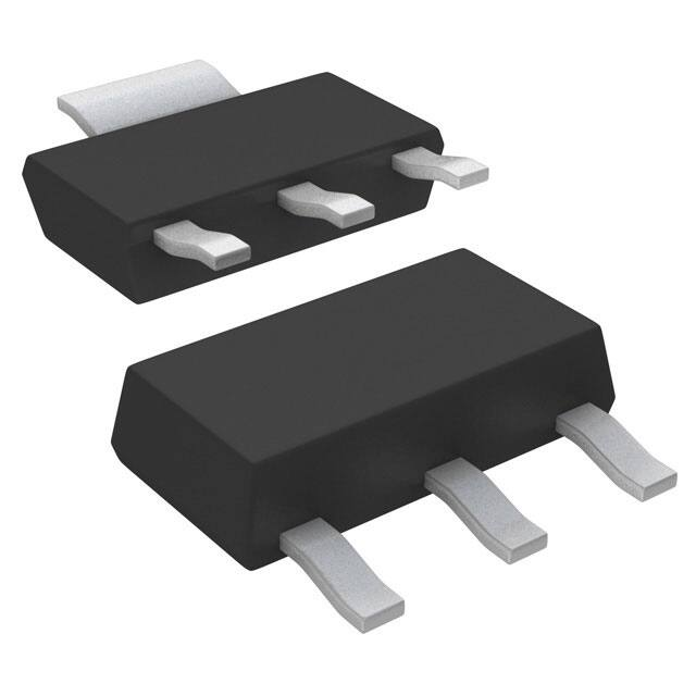
SOT-223,TO-252, TO-220, and TO-263
DESCRIPTION
The SPX1117 is a low power positive-voltage regulator designed to satisfy moderate power
requirements with a cost effective, small footprint solution. This device is an excellent choice for
use in battery-powered applications and portable computers. The SPX1117 features very low
quiescent current and a low dropout voltage of 1.1V at a full load. As output current decreases,
quiescent current flows into the load, increasing efficiency. SPX1117 is available in adjustable
or fixed 1.5V, 1.8V, 2.5V,2.5V, 2.85V, 3.0V, 3.3V and 5V output voltages.
The SPX1117 is offered in several 3-pin surface mount packages: SOT-223, TO-252, TO-220
and TO-263. An output capacitor of 10µF provides unconditional stability while a smaller 2.2µF
capacitor is sufficient for most applications.
FUNCTIONAL DIAGRAM
VIN
+
Current Limit
VOUT
+
ICL
AMP
-
1.25V
VREF
+
Thermal Limit
–
ADJ/GND
IADJ ~ 50µA
–
I TL
Apr 20-07 Rev B
SPX1117 800mA Low Dropout Voltage Regulator
1
© 2007 Sipex Corporation
�ABSOLUTE MAXIMUM RATINGS
Power Dissipation.......................................Internally Limited
Lead Temperature (soldering, 5 seconds) ...............260°C
Storage Temperature Range.......................-65°C to +150°C
Operating Junction Temperature Range.....-40°C to +125°C
Input Supply Voltage .................................................... +20V
Input to Output Voltage ................................................ 18.8V
ESD Rating.................................................................2kV min
These are sterss ratings only and functional operation of the
device at these ratings or any other above those indicated in the
operation sections of the specifications below is not implied.
Exposure to absolute maximum rating conditions for extended
periods of time may affect reliability.
ELECTRICAL CHARACTERISTICS
TA = 25°C, CIN = COUT = 10µF, unless otherwise specified. The Boldface applies over the full operating temperature range.
PARAMETER
CONDITIONS
MIN
TYP
MAX
UNITS
IOUT = 5mA, VIN =3.0V, TJ = 25ºC
5mA ≤ IOUT ≤ 800mA, 2.9V ≤ VIN ≤ 10V
1.485
1.470
1.500
1.515
1.530
V
IOUT = 5mA, VIN =3.3V, TJ = 25ºC
5mA ≤ IOUT ≤ 800mA, 3.2V ≤ VIN ≤ 10V
1.782
1.764
1.800
1.818
1.836
V
IOUT = 5mA, VIN =4.0V, TJ = 25ºC
5mA ≤ IOUT ≤ 800mA, 3.9V ≤ VIN ≤ 10V
2.475
2.450
2.500
2.525
2.550
V
IOUT = 5mA, VIN =4.35V, TJ = 25ºC
5mA ≤ IOUT ≤ 800mA, 4.25V ≤ VIN ≤ 10V
2.821
2.793
2.850
2.878
2.907
V
IOUT = 5mA, VIN =4.5V, TJ = 25ºC
5mA ≤ IOUT ≤ 800mA, 4.4V ≤ VIN ≤ 10V
2.970
2.940
3.000
3.030
3.060
V
IOUT = 5mA, VIN =4.8V, TJ = 25ºC
5mA ≤ IOUT ≤ 800mA, 4.7V ≤ VIN ≤ 10V
3.267
3.234
3.300
3.333
3.366
V
IOUT = 5mA, VIN =6.5V
5mA ≤ IOUT ≤ 800mA, 6.4V ≤ VIN ≤ 12V
4.950
4.90
5
5.050
5.10
V
IOUT=5mA, (VIN - VOUT )= 2V, TJ = 25ºC
5mA≤IOUT≤ 800mA, 1.4V≤(VIN-VOUT)≤ 10V
1.238
1.225
1.250
1.262
1.270
V
1.5V Version
Output Voltage
1.8V Version
Output Voltage
2.5V Version
Output Voltage
2.85V Version
Output Voltage
3.00V Version
Output Voltage
3.30V Version
Output Voltage
5V Version
Output Voltage
All Voltage Options
Reference Voltage
Output Voltage
Temperature Stability
0.3
%
Line Regulation
(Note 1)
VINMIN ≤VIN≤ 12V,VOUT=Fixed/Adj,
IOUT=5mA
3
7
mV
Load Regulation
(Note 1)
5mA≤IOUT≤ 800mA,VOUT=Fixed/Adj
6
12
mV
Dropout Voltage
(Note 2)
IOUT=100mA
IOUT=500mA
IOUT=800mA
1.00
1.05
1.10
1.20
1.25
1.30
V
Quiescent Current
4.25V≤VIN≤ 6.5V
5
10
mA
Apr 20-07 Rev B
SPX1117 800mA Low Dropout Voltage Regulator
2
© 2007 Sipex Corporation
�ELECTRICAL CHARACTERISTICS
TA = 25°C, CIN = COUT = 10µF, unless otherwise specified. The Boldface applies over the full operating temperature range.
PARAMETER
CONDITIONS
MIN
TYP
Adjust Pin Current
Current Limit
(VIN-VOUT)=5V
1.0
50
1.5
120
2.0
µA
A
Thermal Regulation
25°C, 30mS pulse
0.01
0.1
%/W
Ripple Rejection
fRIPPLE=120Hz, (VIN-VOUT)=2V,
VRIPPLE=1VPP
Long Term Stability
RMS Output Noise
60
MAX
UNITS
75
dB
125°C, 1000Hrs
0.03
%
% of VOUT, 10Hz≤f≤10kHz
0.003
%
*Note 1 - For fixed option, VINMIN = VOUT + 1.5V
- For adjustable option, VINMIN = VIN - VOUT = 1.4V
*Note 2 - Dropout voltage is the input voltage minus output voltage that produces a 1% decrease in output voltage with respect
to the nominal output voltage at VIN = VOUT + 1.5V
Apr 20-07 Rev B
SPX1117 800mA Low Dropout Voltage Regulator
3
© 2007 Sipex Corporation
�3.320
3.315
3.310
3.305
3.300
3.295
3.290
3.285
3.280
3.325
3.320
Vout (V)
Output Voltage
TYPICAL PERFORMANCE CHARACTERISTICS
3.315
3.310
3.305
3.300
10
100
4.5
1000
6.5
8.5
1.3
1.2
1.1
1.0
0.9
200
300
400
500
600
700
800
900
1000
1.50
1.00
0.50
0.00
-50
-25
0
25
Indicating Current
Limit Starts
Vout (V)
Output Deviation
(mV)
125
1.27
-100
1.5
Output Current
(A)
100
1.275
0
1.0
V = 4.0V
V =3.3V Fixed
1 =10mA
C =1µF Tan Cap
C =2.2µF Tan Cap
IN
0.5
IN
O
IN
0
OUT
0.2
0.3
0.4 0.5 0.6
Time (ms)
0.7
0.8 0.9
1.265
1.26
1.255
1.25
1.245
1.24
1.235
1.23
1.225
-50
1.25v Adj
-30
1.0
-10
10
30
50
70
90
110
130
Temp (C)
Figure 5. Current Limit for SPX1117M3-3.3, Output
Voltage Deviation with IOUT=10mA to 1A Step
Apr 20-07 Rev B
75
Figure 4. Current Limit for SP1117M3-3.3; VIN=4.8V,
CIN=COUT=1µF, IOUT pulsed from 10mA to Current
Limit
125°C
22µF
0.1
50
Temp ( oC)
Figure 3. Dropout Voltage vs Output Current for
SPX1117M3-3.3; VIN=4.8V, COUT=2.2µF
0
14.5
2.00
Io (mA)
100
12.5
Figure 2. Line Regulation for SPX1117M3-3.3;
IOUT=10mA
Current Limit (A)
Dropout Voltage (V)
Figure 1. Load Regulation for SPX1117M3-3.3;
VIN=4.8V
100
10.5
Vin (V)
Output Current (mA)
Figure 6. VOUT vs Temperature, VIN=2.5V, IOUT=10mA
SPX1117 800mA Low Dropout Voltage Regulator
4
© 2007 Sipex Corporation
�TYPICAL PERFORMANCE CHARACTERISTICS: Continued
1.53
1.84
1.5v Adj
1.5v Fixed
1.52
Vout (V)
Vout (V)
1.5
1.49
1.47
-50
1.8
1.79
1.77
-30
-10
10
30
50
Temp (C)
70
90
110
1.76
-50
130
Figure 7. VIN=3.0V, IOUT=10mA
2.55
2.54
2.53
2.52
2.51
2.5
2.49
2.48
2.47
2.46
2.45
-50
-10
10
70
90
110
2.88
2.86
2.84
2.82
-30
-10
10
30
50
Temp (C)
70
90
110
2.8
-50
130
-30
-10
10
30
50
Temp (C)
70
90
110
130
Figure 10. VIN=4.85V, IOUT=10mA
3.38
3v Adj
3v Fixed
3.04
3.3v Adj
3.3v Fixed
3.36
3.02
Vout (V)
3.34
3
2.98
2.96
3.32
3.3
3.28
-30
-10
10
30
50
70
90
110
3.26
-50
130
-30
-10
10
Temp (C)
30
50
70
90
110
130
Temp (C)
Figure 12. VIN=5.0V, IOUT=10mA
Figure 11. VIN=4.85V, IOUT=10mA
6
4
2
V out, V
0
-2
-4
-6
-8
-40
-20
0
20
40
60
80
100
1.816
1.815
1.814
1.813
1.812
1.811
1.81
1.809
1.808
1.807
1.806
800mA
400mA
10mA
-40
Ambient Temperature,*C
-20
0
20
40
Ambient Temperature, *C
60
80
0.4
0.3
-40°C
0.2
+25°C
0.1
+85°C
0
-0.1
-0.2
-0.3
3
4
5
6
Vin, V
Figure 15. Line Regulation at ILOAD=800mA over
Temperature, VOUT=1.8V adjustable
Apr 20-07 Rev B
100
Figure 14. Output Voltage vs Temperature at different
Current Loads, VIN=3.3V, VOUT = 1.8V Adjustable
Figure 13. Line Regulation vs Temperature. VOUT=1.8V
(adjustable), VIN= 3.3V
Vout tolerance,%
130
2.85v Adj
2.85v Fixed
2.9
3.06
Output Voltage Change, mV
30
50
Temp (C)
2.92
2.5v Adj
2.5v Fixed
Figure 9. VIN=4.0V, IOUT=10mA
2.94
-50
-30
Figure 8. VIN=3.3V, IOUT=10mA
Vout (V)
Vout (V)
1.82
1.81
1.78
1.48
Vout (V)
1.8v Adj
1.8v Fixed
1.83
1.51
SPX1117 800mA Low Dropout Voltage Regulator
5
© 2007 Sipex Corporation
�APPLICATION INFORMATION
Output Capacitor
To ensure the stability of the SPX1117, an
output capacitor of at least 2.2µF (tantalum or
ceramic) or 10µF (aluminum) is required. The
value may change based on the application
requirements of the output load or temperature
range. The value of ESR can vary based on the
type of capacitor used in the applications to
guarantee stability. The recommended value
for ESR is 0.5Ω or less. A larger value of
output capacitance (up to 100µF) can improve
the load transient response.
Soldering Methods
The SPX1117 SOT-223 package is designed
to be compatible with infrared reflow or
vapor-phase reflow soldering techniques.
During soldering, the non-active or mildly
active fluxes may be used. The SPX1117 die
is attached to the heatsink lead which exits
opposite the input, output, and ground pins.
Hand soldering and wave soldering should be
avoided since these methods can cause
damage to the device with excessive thermal
gradients on the package. The SOT-223
recommended soldering method are as
follows: vapor phase reflow and infrared
reflow with the component preheated to within
65°C of the soldering temperature range.
Figure 16. Load Step Response (0 to 800mA), Vin=3.3V,
Vout=1.8V, Cin=10µF, Cout=2.2µF, Ceramic; 1 = Vout,
4= Iload
Figure 17. Load Step Response (0 to 800mA), Vin=3.3V,
Vout=1.8V, Cin=10µF, Cout=2.2µF, OSCON; 1 = Vout,
4= Iload
Apr 20-07 Rev B
SPX1117 800mA Low Dropout Voltage Regulator
6
© 2007 Sipex Corporation
�APPLICATION INFORMATION: Continued
Ripple Rejection
Ripple rejection can be improved by adding a
capacitor between the ADJ pin and ground as
shown in Figure 23. When ADJ pin bypassing
is used, the value of the output capacitor required increases to its maximum. If the ADJ pin
is not bypassed, the value of the output capacitor
can be lowered to 10µF for an electrolytic aluminum capacitor or 2.2µF for a ceramic or solid
tantalum capacitor (Fig 22).
Thermal Characteristics
The thermal resistance of SPX1117 (SOT-223
Package) is 15°C/W from junction to tab and 31
°C/W from tab to ambient for a total of 46 °C/W
from junction to ambient (Table 1). The SPX1117
features the internal thermal limiting to protect
the device during overload conditions. Special
care needs to be taken during continuous load
conditions such that the maximum junction temperature does not exceed 125 °C. Thermal protection is activated at >155°C and deactiviated
at


 工商网监
湘ICP备2023018690号
工商网监
湘ICP备2023018690号
