C4D05120A
VRRM
Silicon Carbide Schottky Diode
IF (TC=135˚C) =
Z-Rec Rectifier
®
Q c
Features
•
•
•
•
•
•
=
27 nC
1.2kV Schottky Rectifier
Zero Reverse Recovery Current
High-Frequency Operation
Temperature-Independent Switching
Extremely Fast Switching
Positive Temperature Coefficient on VF
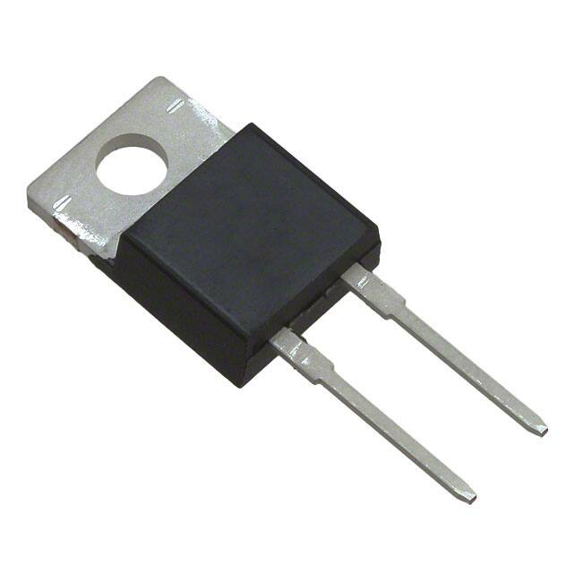
TO-220-2
Replace Bipolar with Unipolar Rectifiers
Essentially No Switching Losses
Higher Efficiency
Reduction of Heat Sink Requirements
Parallel Devices Without Thermal Runaway
PIN 1
Switch Mode Power Supplies (SMPS)
Boost diodes in PFC or DC/DC stages
Free Wheeling Diodes in Inverter stages
AC/DC converters
CASE
PIN 2
Applications
•
•
•
•
9.5 A
Package
Benefits
•
•
•
•
•
= 1200 V
Part Number
Package
Marking
C4D05120A
TO-220-2
C4D05120
Maximum Ratings (TC=25°C unless otherwise specified)
Symbol
Parameter
Unit
Test Conditions
Note
VRRM
Repetitive Peak Reverse Voltage
1200
V
VRSM
Surge Peak Reverse Voltage
1300
V
VR
DC Peak Reverse Voltage
1200
V
IF
Continuous Forward Current
19
9.5
5
A
TC=25˚C
TC=135˚C
TC=161˚C
IFRM
Repetitive Peak Forward Surge Current
26
18
A
TC=25˚C, tP=10 ms, Half Sine Pulse
TC=110˚C, tP=10 ms, Half Sine Pulse
IFSM
Non-Repetitive Forward Surge Current
46
36
A
TC=25˚C, tP=10 ms, Half Sine Pulse
TC=110˚C, tP=10 ms, Half Sine Pulse
Fig. 8
IF,Max
Non-Repetitive Peak Forward Current
400
320
A
TC=25˚C, tP=10 ms, Pulse
TC=110˚C, tP=10 ms, Pulse
Fig. 8
Power Dissipation
100
43
W
TC=25˚C
TC=110˚C
Fig. 4
dV/dt
Diode dV/dt ruggedness
200
V/ns
VR=0-650V
∫i2dt
i2t value
10.6
6.5
A2s
Ptot
TJ
Operating Junction Range
-55 to
+175
˚C
Tstg
Storage Temperature Range
-55 to
+135
˚C
1
8.8
Nm
lbf-in
TO-220 Mounting Torque
1
Value
C4D05120A Rev. C, 09-2016
TC=25˚C, tP=10 ms
TC=110˚C, tP=10 ms
M3 Screw
6-32 Screw
Fig. 3
�Electrical Characteristics
Symbol
Parameter
Typ.
Max.
Unit
VF
Forward Voltage
1.4
1.9
1.8
3
V
IR
Reverse Current
20
40
150
300
QC
Total Capacitive Charge
C
EC
Test Conditions
Note
IF = 5 A TJ=25°C
IF = 5 A TJ=175°C
Fig. 1
μA
VR = 1200 V TJ=25°C
VR = 1200 V TJ=175°C
Fig. 2
27
nC
VR = 800 V, IF = 5A
di/dt = 200 A/μs
TJ = 25°C
Fig. 5
Total Capacitance
390
27
20
pF
VR = 0 V, TJ = 25°C, f = 1 MHz
VR = 400 V, TJ = 25˚C, f = 1 MHz
VR = 800 V, TJ = 25˚C, f = 1 MHz
Fig. 6
Capacitance Stored Energy
8.0
μJ
VR = 800 V
Fig. 7
Note: This is a majority carrier diode, so there is no reverse recovery charge.
Thermal Characteristics
Symbol
RθJC
Parameter
Thermal Resistance from Junction to Case
Typ.
Unit
Note
1.5
°C/W
Fig. 9
Typical Performance
10
1000
9
TJ=-55°C
T = 25°C
TJ= 75°C
J
T =125°C
TJ =175°C
J
8
900
800
700
Current
(µA)
I (μA)
6
5
4
3
500
400
TJ=-55°C
T = 25°C
TJ= 75°C
J
T =125°C
TJ =175°C
J
300
2
200
1
100
0
0
0.5
1
1.5
2
2.5
VF (V)
Voltage
(V)
Figure 1. Forward Characteristics
2
600
R
F
Current
I (A) (A)
7
C4D05120A Rev. C, 09-2016
3
3.5
0
0
500
1000
1500
VR (V)
Voltage (V)
Figure 2. Reverse Characteristics
2000
�Typical Performance
110.0
70
100.0
60
90.0
10%
20%
30%
50%
70%
DC
40
80.0
Duty
Duty
Duty
Duty
Duty
70.0
PTot (W)
IF(peak) (A)
50
30
20
60.0
50.0
40.0
30.0
20.0
10
10.0
0.0
0
25
50
75
100
125
150
175
25
50
75
100
125
150
175
TC ˚C
TC ˚C
Figure 4. Power Derating
Figure 3. Current Derating
35
450
400
30
350
25
300
250
C (pF)
Qc (nC)
20
15
200
150
10
100
5
50
0
0
0
200
400
600
800
0.1
1000
VR (V)
Figure 5. Recovery Charge vs. Reverse Voltage
3
C4D05120A Rev. C, 09-2016
1
10
100
VR (V)
Figure 6. Capacitance vs. Reverse Voltage
1000
�Typical Performance
14
14.0
1000
1000
10.0
10
8.08
(A)
IFSMIFSM
(A)
E (mJ)
C
EC Capacitive Energy (uJ)
12
12.0
6.06
100
100
TJ_intial = 25°C
T
= 110°C
J_intital
4.04
2.02
0.00
0 200 400 600 800 1000
0
200
400
600
800
1000
100
1E-05 1E-04 1E-03 1E-02
1.E-05
1.E-04
1.E-03
1.E-02
VR Reverse
Voltage (V)
V (V)
tptp(s)
(s)
R
Junction
To Case
Impedance,
ZthJC (oC/W)
Thermal
Resistance
(˚C/W)
Figure 7. Typical Capacitance Stored Energy
Figure 8. Non-repetitive peak forward surge current
versus pulse duration (sinusoidal waveform)
1
0.5
0.3
0.1
100E-3
0.05
0.02
SinglePulse
0.01
10E-3
1E-6
10E-6
100E-6
1E-3
Time,
tp (s)
T (Sec)
10E-3
Figure 9. Transient Thermal Impedance
4
C4D05120A Rev. C, 09-2016
100E-3
1
�Package Dimensions
Package TO-220-2
POS
PIN 1
PIN 2
CASE
Inches
Millimeters
Min
Max
Min
Max
A
.381
.410
9.677
10.414
6.477
B
.235
.255
5.969
C
.100
.120
2.540
3.048
D
.223
.337
5.664
8.560
D1
.457-.490
11.60-12.45 typ
D2
.277-.303 typ
7.04-7.70 typ
D3
.244-.252 typ
6.22-6.4 typ
E
.590
.615
14.986
15.621
E1
.302
.326
7.68
8.28
E2
.227
251
5.77
6.37
F
.143
.153
3.632
3.886
G
1.105
1.147
28.067
29.134
H
.500
.550
12.700
13.970
L
.025
.036
.635
.914
M
.045
.055
1.143
1.550
N
.195
.205
4.953
5.207
P
.165
.185
4.191
4.699
Q
.048
.054
1.219
1.372
S
3°
6°
3°
6°
6°
T
3°
6°
3°
U
3°
6°
3°
6°
V
.094
.110
2.388
2.794
W
.014
.025
.356
.635
X
3°
5.5°
3°
5.5°
Y
.385
.410
9.779
10.414
z
.130
.150
3.302
3.810
NOTE:
1. Dimension L, M, W apply for Solder Dip Finish
Recommended Solder Pad Layout
TO-220-2
Part Number
Package
Marking
C4D05120A
TO-220-2
C4D05120
Note: Recommended soldering profiles can be found in the applications note here:
http://www.wolfspeed.com/power_app_notes/soldering
5
C4D05120A Rev. C, 09-2016
�Diode Model
VfT = VT + If * RT
VT = 0.96 + (Tj * -1.22*10-3)
RT = 0.08 + (Tj * 8.5*10-4)
Note: Tj is diode junction temperature in degrees Celsius
Notes
• RoHS Compliance
The levels of RoHS restricted materials in this product are below the maximum concentration values (also referred
to as the threshold limits) permitted for such substances, or are used in an exempted application, in accordance
with EU Directive 2011/65/EC (RoHS2), as implemented January 2, 2013. RoHS Declarations for this product can
be obtained from your Wolfspeed representative or from the Product Ecology section of our website at http://
www.wolfspeed.com/power/tools-and-support/product-ecology.
• REACh Compliance
REACh substances of high concern (SVHCs) information is available for this product. Since the European Chemical Agency (ECHA) has published notice of their intent to frequently revise the SVHC listing for the foreseeable
future,please contact a Cree representative to insure you get the most up-to-date REACh SVHC Declaration.
REACh banned substance information (REACh Article 67) is also available upon request.
•
This product has not been designed or tested for use in, and is not intended for use in, applications implanted into
the human body nor in applications in which failure of the product could lead to death, personal injury or property
damage, including but not limited to equipment used in the operation of nuclear facilities, life-support machines,
cardiac defibrillators or similar emergency medical equipment, aircraft navigation or communication or control
systems, or air traffic control systems.
Related Links
•
•
•
Cree SiC Schottky diode portfolio: http://www.wolfspeed.com/Power/Products#SiCSchottkyDiodes
Schottky diode Spice models: http://www.wolfspeed.com/power/tools-and-support/DIODE-model-request2
SiC MOSFET and diode reference designs: http://go.pardot.com/l/101562/2015-07-31/349i
Copyright © 2016 Cree, Inc. All rights reserved.
The information in this document is subject to change without notice.
Cree, the Cree logo, and Zero Recovery are registered trademarks of Cree, Inc.
6
C4D05120A Rev. C, 09-2016
Cree, Inc.
4600 Silicon Drive
Durham, NC 27703
USA Tel: +1.919.313.5300
Fax: +1.919.313.5451
www.cree.com/power
�


 工商网监
湘ICP备2023018690号
工商网监
湘ICP备2023018690号
