TS2596
Taiwan Semiconductor
3A / 150kHz Step-Down DC-DC Converter
GENERAL DESCRIPTION
FEATURES
The TS2596 Series are step-down switching regulators
● Output voltage: 3.3V, 5V & adjustable version
with all required active functions. It is capable of driving
● Adjustable output voltage range 1.23V~38.5V
3A load with excellent line and load regulations. These
● 150kHz fixed switching frequency
devices are available in fixed output voltages of 3.3V, 5V,
● Voltage mode Non-synchronous PWM control
and an adjustable output version.
● Thermal shutdown and current limit protection
The TS2596 series operates at a switching frequency of
● ON/OFF shutdown control input
150kHz thus allowing smaller sized filter components than
● Short circuit protect (SCP)
what would be needed with lower frequency switching
● Operating voltage can be up to 40V
regulators. It substantially not only reduces the area of
● Output load current 3A
board size but also the size of heat sink, and in some
● Low power standby mode
cases no heat sink is required. The ±4% tolerance on
frequency accuracy is within ±10%. External shutdown is
● Built-in switching transistor on chip
● Compliant to RoHS Directive 2011/65/EU and in
accordance to WEEE 2002/96/EC.
● Halogen-free according to IEC 61249-2-21
included. Featuring 100μA (typical) standby current. The
APPLICATION
output switch includes cycle-by-cycle current limiting, as
● Simple High-efficiency Step down Regulator
well as thermal shutdown for full protection under fault
● On-Card Switching Regulators
conditions.
● Positive to Negative Converter
output voltage within specified input voltages and output
load conditions is guaranteed. Also, the oscillator
2
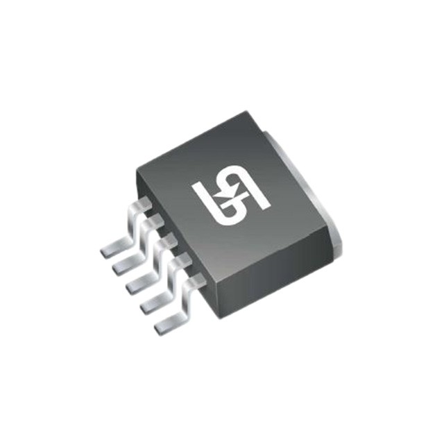
TO-263-5L (D PAK)
Pin Definition:
1. Input
2. SW Output
3. Ground
4. Feedback
5. Enable
Notes: Moisture sensitivity level: level 3. Per J-STD-020
TYPICAL APPLICATIN CIRCUIT
Adjustable Output Voltage Version
VOUT = VFB × (1 + R1 ), VFB = 1.23V, R2 = 0.7k ~ 3k
R2
1
Version: G1608
�TS2596
Taiwan Semiconductor
ABSOLUTE MAXIMUM RATINGS
PARAMETER
SYMBOL
LIMIT
UNIT
Maximum Supply Voltage
VCC
+45
V
Recommend Operating Supply Voltage
VOP
+4.5 to +40
V
VSW , VEN
-0.3 to +40
V
Feedback Pin Voltage
VFB
-0.3 to +12
V
Power Dissipation
PD
Internally Limited
W
VOUT
-1
V
Storage Temperature Range
TST
-65 ~ +150
°C
Operating Temperature Range
TOP
-40 ~ +125
°C
2
kV
SYMBOL
LIMIT
UNIT
Junction to Case Thermal Resistance
RӨJC
2
°C/W
Junction to Ambient Thermal Resistance
RӨJA
50
SW, EN Pin Input Voltage
Output Voltage to Ground
ESD Susceptibility (HBM)
THERMAL INFORMATION
PARAMETER
°C/W
2
Note: RӨJA is measured with the PCB copper area (need connect to GROUND pins) of approximately 1.5 in (Multi-layer)
ELECTRICAL CHARACTERISTICS
(VIN = 12V for 3.3V, 5V, Adjustable Version, ILOAD = 0.3A, TA = 25°C unless otherwise noted)
PARAMETER
CONDITION
Output Feedback
ADJ
Efficiency
Output Feedback
3.3V
4.5V ≤ VIN ≤ 40V
0.2A ≤ ILOAD ≤ 3A
VIN = 12V, ILOAD = 3A,
VOUT = 5V
4.75V ≤ VIN ≤ 40V
0.2A ≤ ILOAD ≤ 3A
Efficiency
VIN = 12V, ILOAD = 3A
Output Feedback
7V ≤ VIN ≤ 40V
0.2A ≤ ILOAD ≤ 3A
5V
SYMBOL
MIN
TYP
MAX
UNIT
VFB
1.180
1.23
1.280
V
η
--
77
--
%
VFB
3.135
3.3V
3.465
V
η
--
75
--
%
VFB
4.75
5
5.25
V
Efficiency
VIN = 12V, ILOAD = 3A
η
--
80
--
%
Feedback Bias Current
VFB =1.3V (Adj version only)
IFB
--
10
100
nA
FOSC
127
150
173
kHz
Oscillator Frequency
Soft-Start Time
Rising edge of EN on to ICL
TSS
--
3
--
ms
Current Limit
Pear Current, no outside circuit
VFB =0V force driver on
ICL
3.3
--
--
A
When current limit occurred
o
and VFB
很抱歉,暂时无法提供与“TS2596CM5 RNG”相匹配的价格&库存,您可以联系我们找货
免费人工找货- 国内价格 香港价格
- 1+20.204781+2.61030
- 5+17.055995+2.20350
- 10+15.4815910+2.00010
- 25+13.5573225+1.75150
- 100+11.89546100+1.53680
- 800+10.84586800+1.40120
- 国内价格 香港价格
- 800+11.86524800+1.53290
- 1600+11.543521600+1.49134
- 2400+11.382402400+1.47052
- 4000+11.203914000+1.44746
- 5600+11.099575600+1.43398
- 8000+10.999298000+1.42103
- 国内价格 香港价格
- 1+21.924051+2.83242
- 10+16.2746810+2.10257
- 25+14.8579025+1.91953
- 100+13.30761100+1.71924
- 250+12.56788250+1.62368
- 国内价格 香港价格
- 800+9.56735800+1.23603
- 4800+9.239844800+1.19372