Advanced Science And Novel Technology Company, Inc.
2790 Skypark Drive Suite 112, Torrance, CA 90505
Offices: 310-530-9400 / Fax: 310-530-9402
www.adsantec.com
ASNT8051-PQB
9.9-12.1GHz and 11-12.9GHz Programmable PLL with integrated VCOs
nc
vee
vee
phs2
phs1
nc
vcc
clop
vcc
clon
vcc
vcc
vcc
chop
vcc
chon
ASNT8051
vcc
vcc
1
vee
off12g
offpll
ftr1n
vee
ftr1p
vcc
loln
vcc
offcho
cen
vee
vcc
offecl
cep
cr16n
vcc
cr16p
Rev. 1.5.2
vcc
vcc
vecl
Programmable clock multiplier (CMU) with two selectable frequency ranges of internal PLL
Optional operational mode as a clock divider with PLL disabled
Closed-Loop SSB phase noise at 10MHz offset better than 98dB/Hz
On-chip Loss-of-Lock control circuit
External RC loop filter
LVDS, CML, or PECL input reference clock interface
Full-rate CML clock input interface
Full-rate or half-rate CML clock output interface
LVDS divided clock output with optional 90°-step phase adjustment
Single +3.3V power supply
Low power consumption of 570mW
Fabricated in SiGe for high performance, yield, and reliability
Standard 40-pin QFN package
vee
February 2020
�Advanced Science And Novel Technology Company, Inc.
2790 Skypark Drive Suite 112, Torrance, CA 90505
Offices: 310-530-9400 / Fax: 310-530-9402
www.adsantec.com
DESCRIPTION
ce
offpll
off12g
loln
ftr1p
ftr1n
vecl
cr16
offecl
offcho
HS
CIB
PLL
/16
LS
CIB
CPR
phs1
phs2
LS
COB
clo
HS
COB
cho
C2
ref
C
Fig. 1. Functional Block Diagram
ASNT8051-PQB is a clock multiplication unit (CMU) with a dual-range phase-locked loop (PLL)
incorporating high-speed voltage-controlled oscillators (VCOs). The part features several control
functions shown in Table 1. All functions are further described in the specified sections.
Table 1. PLL Control Functions
Control
Logic State
Described
signal
in.
Not connected (default)
“0”
“1”
Higher VCO range
Same as 0 state
Lower VCO range
PLL
off12g
Full-rate HS output clock Half-rate HS output clock HS COB disabled HS COB
offcho
See Table 4
CPR
phs1/phs2
PLL enabled
Same as 0 state
PLL disabled
PLL
offpll
CML/PECL input interface
Same as 1 state
LVDS input interface LS CIB
offecl
One of the two frequency ranges can be selected by the control signal off12g. In the main operational
mode, the IC shown in Fig. 1 accepts a low-speed reference clock cr16p/cr16n with the frequency f/16
and converts it into a high-speed output clock cho with the selectable frequency f or f/2 and a low-speed
output clock clo with the frequency f/16. The frequency of the high-speed clock is selected through the
external 3-state control signal offcho that can also disable the clock output buffer.
One of four 90° shifted phases of the low-speed output clock with the frequency f/16 can be selected by
control signals phs1 and phs2.
When operating in the closed-loop mode, the PLL requires an external loop filter connected to pins ftr1p
and ftr1n. The output signal loln indicates the locked or unlocked state of the PLL. The PLL also supports
an open-loop mode of operation with its selected VCO controlled externally by voltages applied to the
filter pins ftr1p and ftr1n. The chip can operate as a divider by 16 of the input high-speed clock cep/cen
if the PLL is disabled by the control signal offpll.
Rev. 1.5.2
2
February 2020
�Advanced Science And Novel Technology Company, Inc.
2790 Skypark Drive Suite 112, Torrance, CA 90505
Offices: 310-530-9400 / Fax: 310-530-9402
www.adsantec.com
The IC uses a single +3.3V power supply and is characterized for operation from −25°C to 125°C of
junction temperature.
HS CIB
The High-Speed Clock Input Buffer (HS CIB) can process an external clock signal cep/cen with
frequencies from DC to the specified maximum value. The clock inputs support the CML logic interface
with on chip 50Ohm termination to vcc and may be used differentially, AC/DC coupled, single-ended, or
in any combination. In the DC-coupling mode, the input signal’s common mode voltage should comply
with the specifications shown in ELECTRICAL CHARACTERISTICS. In the AC-coupling mode, the
input termination provides the required common mode voltage automatically. The differential DC
signaling mode is recommended for optimal performance.
LS CIB
The Low-Speed Clock Input Buffer (LS CIB) is a proprietary universal input buffer (UIB) that can run at
a high frequency. The UIB’s input termination impedance is controlled by the CMOS signal offecl and is
set to 100Ohm differential if offecl=”1” (true LVDS mode, default state) or 50Ohm single-ended to vecl
if offecl=”0” (CML mode). The value of vecl should be equal to vcc in CML mode. It can be also set to
vcc-2V in order to support the PECL interface. In this case, the corresponding termination voltage source
should be able to both sink and source up to 20mA of current. Possible input clock application schemes
are detailed in Table 2, where Vcm is the common-mode voltage of the clock signal.
Table 2. LS Input Clock Application Schemes
Interface
type
LVDS
(offecl
=1)
CML or
PECL
(offecl
=0)
Clock
cr16p signal
type Swing, mV Connection
Vcm, V
Diff. 70-to-500
DC
1.2±1.0
SE 140-to-900
AC
Threshold
DC
vee-to-vcc
Diff. 70-to-500
DC
vcc-Swing/2
AC
SE 140-to-900
AC
140-to-900
AC
Not connected
Threshold
DC
vcc
Swing, mV
70-to-500
Threshold
140-to-900
70-to-500
Threshold
140-to-900
140-to-900
cr16n signal
Connection
Vcm, V
DC
1.2±1.0
DC
vee-to-vcc
AC
DC
vcc-Swing/2
AC
Not connected
DC
vcc
AC
AC
-
As can be seen, the UIB is designed to accept differential signals with DC common mode voltages
between the negative (vee) and the positive (vcc) supply rails, as well as AC common mode noise with a
frequency up to 5MHz and voltage levels from vee to vee+2.4V. It can also receive single-ended signals
with a threshold voltage between vee and vcc applied to the unused pin of the differential input interface.
PLL
The PLL contains a phase frequency detector, a charge pump, an on-chip integrator with an additional offchip filter connected between pins ftr1p and ftr1n, and two selectable LC-tank VCOs with different
central frequencies. The recommended parameters of the external filter schematic components shown in
Fig. 2 are for reference only and can be modified based on specific requirements.
Rev. 1.5.2
3
February 2020
�Advanced Science And Novel Technology Company, Inc.
2790 Skypark Drive Suite 112, Torrance, CA 90505
Offices: 310-530-9400 / Fax: 310-530-9402
www.adsantec.com
Fig. 2. External Filter Schematic
The PLL is activated by the external control signal offpll=”0” (default state). In case of offpll=”1”, the
PLL is disabled and the chip operates as a divider by 16.
The main function of the PLL is to synthesize the full-rate clock C by aligning the phase and frequency of
the divided clock from the internal divider to the externally applied reference clock cr16. Selection of the
required VCO is defined by the CMOS control signal off12g (lower-speed VCO if off12g=”1”; higherspeed VCO if off12g=”0”, default state). The state of the PLL is indicated by the output CMOS loss-oflock alarm signal loln (loln=”0” if PLL is not locked, loln=”1” if phases and frequencies of internal and
reference clocks are matching).
If required, the selected VCO can be externally controlled by voltages applied to pins ftr1p and ftr1n as
shown in Table 3. In this case, the PLL is operating in the open-loop mode. The unused VCO is
completely disabled in order to save power.
Table 3. VCO External Control Modes
ftr1p signal, V
Vccm+0.8=3.1
Vccm-0.8=1.5
Vccm=2.3
Vccm=2.3
ftr1n signal, V VCO frequency
Vccm=2.3
min
Vccm=2.3
max
Vccm+0.8=3.1
max
Vccm-0.8=1.5
min
Divider-by-16
The Divider-by-16 (/16) includes 4 divide-by-2 circuits connected in series. The clocks divided by 8 and
16 are supplied to the PLL’s phase detector and to the clock processor CPR.
CPR
The clock processor (CPR) receives divided by 16 clocks from the divider and supplies the processed
signal to the low-speed clock output buffer LS COB. The phase of the delivered divided-by-16 clock C16
can be altered utilizing the CMOS control pins phs1 and phs2 as shown in Table 4.
Table 4. Output Clock Phase Selection
phs1
phs2
C16 phase
vee (default) vee (default)
0°
90°
vee
vcc
180°
vcc
vee
270°
vcc
vcc
Rev. 1.5.2
4
February 2020
�Advanced Science And Novel Technology Company, Inc.
2790 Skypark Drive Suite 112, Torrance, CA 90505
Offices: 310-530-9400 / Fax: 310-530-9402
www.adsantec.com
HS COB
The High Speed Clock Output Buffer (HS COB) receives full-rate (C) and half-rate (C2) clocks from the
PLL and converts the selected one into CML output signal cho. The state of the buffer is controlled by
the external CMOS control signal offcho (disabled if offcho=”1”; C2 output if offcho is not connected,
default state; C output if offcho=”0”).
LS COB
The LVDS Low-Speed Clock Output Buffer (LS COB) converts the signal from the CPR into the LVDS
output signal clo. The proprietary low-power LVDS output buffer utilizes a special architecture that
ensures operation at frequencies up to 2.0GHz with a low power consumption level of 30mW. The buffer
satisfies all requirements of the IEEE Std. 1596.3-1996 and ANSI/TIA/EIA-644-1995. For the correct
operation, it requires external differential 100Ohm DC termination at the receiver side. These pins should
NEVER be CONNECTED to devices with 50Ohm termination to ground WITHOUT DC BLOCKS!
ABSOLUTE MAXIMUM RATINGS
Caution: Exceeding the absolute maximum ratings shown in Table 5 may cause damage to this product
and/or lead to reduced reliability. Functional performance is specified over the recommended operating
conditions for power supply and temperature only. AC and DC device characteristics at or beyond the
absolute maximum ratings are not assumed or implied. All min and max voltage limits are referenced to
ground (assumed vee).
Table 5. Absolute Maximum Ratings
Parameter
Supply Voltage (vcc)
Power Consumption
RF Input Voltage Swing (SE)
Case Temperature
Storage Temperature
Operational Humidity
Storage Humidity
Rev. 1.5.2
Min
Max
3.6
0.63
1.0
+90
+100
98
98
-40
10
10
5
Units
V
W
V
ºC
ºC
%
%
February 2020
�Advanced Science And Novel Technology Company, Inc.
2790 Skypark Drive Suite 112, Torrance, CA 90505
Offices: 310-530-9400 / Fax: 310-530-9402
www.adsantec.com
TERMINAL FUNCTIONS
TERMINAL
Name
No. Type
cep
cen
chop
chon
14
13
17
16
cr16p
cr16n
clop
clon
1
2
20
19
offecl
offcho
off12g
offpll
phs2
phs1
ftr1p
ftr1n
loln
3
5
9
11
24
25
7
8
6
Name
vcc
vee
nc
Rev. 1.5.2
DESCRIPTION
High-Speed I/Os
Input CML differential external clock inputs with internal SE 50Ohm
termination to vcc
Output CML differential clock outputs with internal SE 50Ohm termination
to vcc. Require external SE 50Ohm termination to vcc
Low-Speed I/Os
Input LVDS/CML clock inputs. See LS CIB for allowed application
schemes
Output LVDS clock outputs. See LS COB for a detailed description
Input
Controls
3.3V CMOS control signals
Input
Pins for connecting the external loop filter. Can be also used for VCO
external control in the open-loop mode
Output 3.3V CMOS control output
Supply and Termination Voltages
Description
Pin Number
Positive power supply (+3.3V )
12, 15, 18, 27, 28, 29, 31, 32, 33, 34, 35, 36, 37,
38, 39
External ground (0V )
4, 10, 22, 23, 30, 40
Not connected pins
21, 26
6
February 2020
�Advanced Science And Novel Technology Company, Inc.
2790 Skypark Drive Suite 112, Torrance, CA 90505
Offices: 310-530-9400 / Fax: 310-530-9402
www.adsantec.com
ELECTRICAL CHARACTERISTICS
PARAMETER
TYP MAX
UNIT
COMMENTS
General Parameters
0.0
V
External ground
vee
3.1
3.3
3.5
V
±6%
vcc
Ivcc
165
180
mA
Power consumption
570
mW
Junction temperature
-40
25
125
°C
HS Input Clock (cep/cen)
Frequency
DC
17
GHz
Swing
220
800
mV
Differential or SE, p-p, at 17GHz
50
800
mV
Differential or SE, p-p, at 4GHz
CM Voltage Level
vcc-0.8
vcc
V
Must match for both inputs
Duty Cycle
40%
50%
60%
LS Input Clock (cr16p/cr16n)
Frequency
DC
810
MHz
Swing
140
900
mV
Differential or SE, p-p
CM Voltage Level
vee
1.6
vcc
V
Must match for both inputs
HS Output Clock (chop/chon)
Frequency
DC
17
GHz
Logic “1” level
V
vcc
Logic “0” level
vcc-0.58
V
Jitter
6
ps
Peak-to-peak at 12.5GHz
Duty Cycle
50%
LS Output Clock (clop/clon)
Frequency
DC
1060
MHz
Interface
LVDS
Meets the IEEE Std.
CMOS control inputs and outputs (offecl, offcho, off12g, offpll, oncml, phs1, phs2, loln)
Logic “1” level
vcc-0.3
V
Logic “0” level
vee+0.3
V
VCOs
Low frequency of VCO 1
11.0
GHz
Higher-speed VCO.
Active if off12g =”0”
High frequency of VCO 1
12.9
GHz
Low frequency of VCO 2
9.9
GHz
Lower-speed VCO.
Active if off12g =”1”
High frequency of VCO 2
12.1
GHz
External control common
2.3
V
In the open-loop mode
mode vccm
External control voltage vccm-0.8
vccm+0.8
V
In the open-loop mode
range
Rev. 1.5.2
MIN
7
February 2020
�Advanced Science And Novel Technology Company, Inc.
2790 Skypark Drive Suite 112, Torrance, CA 90505
Offices: 310-530-9400 / Fax: 310-530-9402
www.adsantec.com
PACKAGE INFORMATION
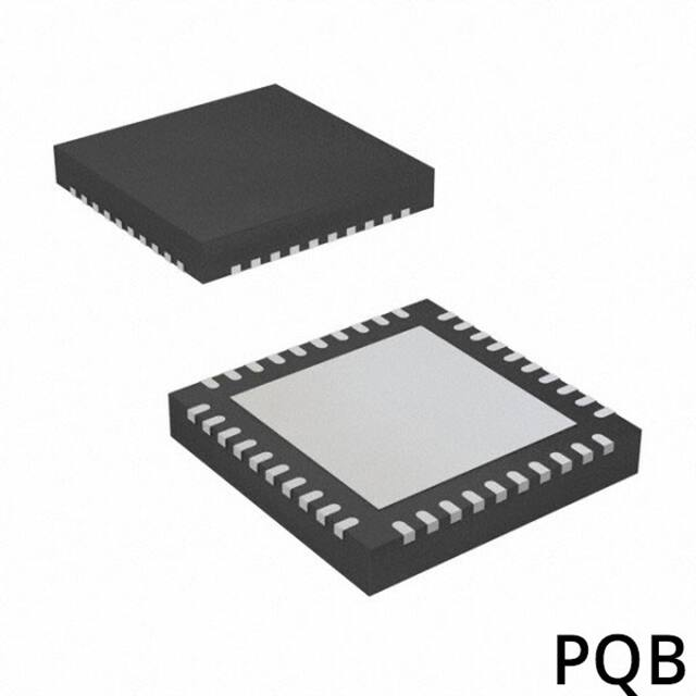
The chip is packaged in a standard 40-pin QFN package shown Fig. 3. It is recommended that the center
heat slug located on the back side of the package is soldered to the vee plain that is ground for the
positive supply.
The part’s identification label is ASNT8051-PQB. The first 8 characters of the name before the dash
identify the bare die including general circuit family, fabrication technology, specific circuit type, and part
version while the 3 characters after the dash represent the package’s manufacturer, type, and pin out
count.
This device complies with the Restriction of Hazardous Substances (RoHS) per 2011/65/EU for all ten
substances.
ASNT8051
Fig. 3. Package Drawing
Rev. 1.5.2
8
February 2020
�Advanced Science And Novel Technology Company, Inc.
2790 Skypark Drive Suite 112, Torrance, CA 90505
Offices: 310-530-9400 / Fax: 310-530-9402
www.adsantec.com
REVISION HISTORY
Revision
1.5.2
1.4.2
1.4.1
1.3.1
1.2.1
Date
02-2020
07-2019
08-2015
05-2013
03-2013
1.1
1.0
05-2012
04-2012
Rev. 1.5.2
Changes
Updated Package Information
Updated Letterhead
Updated Fig. 2 External Filter Schematic
Corrected clock names in Table 2
Revised title
Corrected description
Corrected electrical characteristics
Updated format
Corrected supply information
First release
9
February 2020
�


 工商网监
湘ICP备2023018690号
工商网监
湘ICP备2023018690号
