CGHV1F006S
6 W, DC - 15 GHz, 40 V, GaN HEMT
Description
Cree’s CGHV1F006S is an unmatched, gallium nitride (GaN) high electron mobility
transistor (HEMT) designed specifically for high efficiency, high gain and wide
bandwidth capabilities. The device can be deployed for L, S, C, X and Ku-Band
amplifier applications. The datasheet specifications are based on a C-Band (5.5
- 6.5 GHz) amplifier. Additional application circuits are available for C-Band at
5.8 GHz - 7.2 GHz and X-Band at 7.9 - 8.4 GHz and 8.5 - 9.6 GHz. The CGHV1F006S
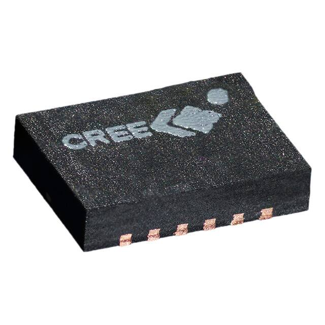
operates on a 40 volt rail circuit while housed in a 3mm x 4mm, surface mount,
dual-flat-no-lead (DFN) package. Under reduced power, the transistor can operate
below 40V to as low as 20V VDD, maintaining high gain and efficiency.
Package Type: 3x4 DFN
PN: CGHV1F006S
Typical Performance Over 5.5 - 6.5 GHz (TC = 25˚C), 40 V
Parameter
5.5 GHz
6.0 GHz
6.5 GHz
Units
Small Signal Gain
15.4
16.5
17.8
dB
Output Power @ PIN = 28 dBm
38.6
39.3
39.0
dBm
Drain Efficiency @ PIN = 28 dBm
55
57
52
%
Note: Measured in the CGHV1F006S-AMP application circuit. Pulsed 100 μs 10% duty
Features for 40 V in CGHV1F006S-AMP
•
•
•
•
Up to 15 GHz Operation
8 W Typical Output Power
17 dB Gain at 6.0 GHz
15 dB Gain at 9.0 GHz
•
•
Application circuits for 5.8 - 7.2 GHz, 7.9 - 8.4
GHz, and 8.5 - 9.6 GHz.
High degree of APD and DPD correction can
be applied
Listing of Available Hardware Application Circuits / Demonstration Circuits
Application Circuit
Operating Frequency
Amplifier Class
Operating Voltage
CGHV1F006S-AMP1
5.85 - 7.2 GHz
Class A/B
40 V
CGHV1F006S-AMP2
7.9 - 8.4 GHz
Class A/B
40 V
CGHV1F006S-AMP3
8.5 - 9.6 GHz
Class A/B
40 V
CGHV1F006S-AMP4
4.9 - 5.9 GHz
Class A/B
20 V
Large Signal Models Available for ADS and MWO
Rev 5.7 – May 2021
4600 Silicon Drive | Durham, NC 27703 | wolfspeed.com
�CGHV1F006S
2
Absolute Maximum Ratings (not simultaneous) at 25˚C Case Temperature
Parameter
Symbol
Rating
Units
Notes
Drain-Source Voltage
VDSS
120
Volts
25˚C
Gate-to-Source Voltage
VGS
-10, +2
Volts
25˚C
Storage Temperature
TSTG
-65, +150
˚C
Operating Junction Temperature
TJ
225
˚C
Maximum Forward Gate Current
IGMAX
1.2
mA
25˚C
Maximum Drain Current
IDMAX
0.95
A
25˚C
TS
245
˚C
TC
-40, +150
˚C
RθJC
14.5
˚C/W
1
Soldering Temperature
2
Case Operating Temperature
3,4
Thermal Resistance, Junction to Case5
Notes:
1
Current limit for long term, reliable operation
2
Refer to the Application Note on soldering
at wolfspeed.com/rf/document-library
3
Simulated at PDISS = 2.4 W
4
TC = Case temperature for the device. It refers to the temperature at the
ground tab underneath the package. The PCB will add additional
thermal resistance
5
85˚C
The RTH for Cree’s application circuit, CGHV1F006S-AMP, with 31
(Ø11 mil) via holes designed on a 20 mil thick Rogers 5880 PCB, is
3.9°C/W. The total RTH from the heat sink to the junction is
14.5°C/W + 3.9°C/W = 18.4°C/W
Electrical Characteristics (TC = 25˚C), 40 V Typical
Characteristics
Symbol Min.
Typ.
Max.
Units
Conditions
Gate Threshold Voltage
VGS(th)
-3.6
-3.0
-2.4
VDC
VDS = 10 V, ID = 1.2 mA
Gate Quiescent Voltage
VGS(Q)
–
-2.7
–
VDC
VDS = 40 V, ID = 60 mA
Saturated Drain Current2
IDS
0.86
1.2
–
A
VDS = 6.0 V, VGS = 2.0 V
Drain-Source Breakdown Voltage
V(BR)DSS
100
–
–
VDC
VGS = -8 V, ID = 1.2 mA
DC Characteristics
1
RF Characteristics (TC = 25˚C, F0 = 5.925 GHz unless otherwise noted)
3
Small Signal Gain3,4
G
15.15
17.4
-
dB
VDD = 40 V, IDQ = 60 mA, PIN = 10 dBm
Output Power
POUT
37.5
38.7
–
dBm
VDD = 40 V, IDQ = 60 mA, PIN = 25.5 dBm
η
35
52
-
%
VDD = 40 V, IDQ = 60 mA, PIN = 25.5 dBm
VSWR
-
10 : 1
-
Y
No damage at all phase angles,
VDD = 40 V, IDQ = 60 mA, PIN = 25.5 dBm
CGS
–
1.3
–
pF
VDS = 40 V, Vgs = -8 V, f = 1 MHz
Output Capacitance
CDS
–
0.31
–
pF
VDS = 40 V, Vgs = -8 V, f = 1 MHz
Feedback Capacitance
CGD
–
0.04
–
pF
VDS = 40 V, Vgs = -8 V, f = 1 MHz
3,4
Drain Efficiency
3,4
Output Mismatch Stress4
Dynamic Characteristics
Input Capacitance5
5
Notes:
1
Measured on wafer prior to packaging
2
Scaled from PCM data
3
Measured in Cree’s production test fixture. This fixture is designed for high volume testing at 5.925 GHz
4
Unmodulated Pulsed Signal 100 μs, 10% duty cycle
5
Includes package
Rev 5.7 – May 2021
4600 Silicon Drive | Durham, NC 27703 | wolfspeed.com
�CGHV1F006S
3
Electrical Characteristics When Tested in CGHV1F006S-AMP1 at C-Band Under OQPSK
Characteristics
Symbol
Min.
Typ.
Max.
Units
Conditions
RF Characteristics1 (TC = 25˚C, F0 = 5.8 - 7.2 GHz unless otherwise noted)
Gain
G
–
17.5
–
dB
VDD = 40 V, IDQ = 60 mA, PIN = 0 dBm
Output Power2
POUT
–
39
–
dBm
VDD = 40 V, IDQ = 60 mA, PIN = 27 dBm
Drain Efficiency2
η
–
55
–
%
VDD = 40 V, IDQ = 60 mA, PIN = 27 dBm
OQPSK3
ACLR
–
-36
–
dBc
VDD = 40 V, IDQ = 60 mA, POUT = 33 dBm
Output Mismatch Stress2
VSWR
–
10:1
–
Y
No damage at all phase angles, VDS = 40 V, IDQ
= 60 mA
Notes:
1
Measured in CGH1F006S-AMP1 Application Circuit
2
Pulsed 100 μs, 10% duty cycle
3
OQPSK modulated signal, 1.6 msps, PN23, Alpha Filter = 0.2 Offset = 1.6 MHz
Typical Performance - CGHV1F006S-AMP1 at C-Band Under OQPSK
Figure 1. Typical Small Signal Response of CGHV1F006S-AMP1 Application Circuit
VDD = 40 V, IDQ = 60 mA
30
Magnitude (dB)
Magnitude (dB)
20
10
0
-10
-20
S11
S21
S22
-30
5.0
5.5
6.0
6.5
Frequency (GHz)
7.0
7.5
8.0
Frequency (GHz)
Rev 5.7 – May 2021
4600 Silicon Drive | Durham, NC 27703 | wolfspeed.com
�CGHV1F006S
4
Typical Performance in Application Circuit CGHV1F006S-AMP1
Figure 2. Typical Gain, Efficiency and OQPSK Performance vs Frequency
POUT = 33 dBm. VDD = 40 V, IDQ = 60 mA
CGHV1F006S OQPSK Performance at 33dBm
40
0
Efficiency
Gain
30
-10
25
-15
20
-20
Gain
15
-25
10
-30
OQPSK Offset (dBc)
Gain (dB) and Efficiency (%)
Gain (dB) and Efficiency (%)
-5
Efficiency
Offset
OQPSK Offset (dBc)
35
Offset
5
0
-35
5.8
6.0
6.2
6.4
6.6
Frequency (GHz)
6.8
7.0
7.2
-40
Frequency (GHz)
CGHV1F006S OQPSK Transfer @ 7.2GHz
Figure 3. Typical Gain, Efficiency and OQPSK Performance vs Input Power OQPSK Transfer
Frequency = 7.2 GHz, VDD = 40 V, IDQ = 60 mA
35
-15
DEff
30
-20
Gain_
Gain
Gain(dB)
(dB)
Efficiency(%)
(%)
Efficiency
25
+Oset_
20
-25
Efficiency
-30
Gain
15
-35
Offset
10
-40
5
-45
0
10
15
20
25
30
35
OQPSK
Offset
(dBc)
OQPSK
Offset
(dBc)
-Oset_
-50
InputPower
Power (dBm)
Input
(dBm)
Rev 5.7 – May 2021
4600 Silicon Drive | Durham, NC 27703 | wolfspeed.com
�CGHV1F006S
5
Typical Performance in Application Circuit CGHV1F006S-AMP1
Drain Efficiency (%)
Output Power (dBm)
Figure 4. Typical Pulsed Power Response
VDD = 40 V, IDQ = 60 mA, 100 μs, 10% Duty, PIN = 27 dBm
Frequency (GHz)
CGHV1F006S-AMP1 Application Circuit
Bill of Materials, OQPSK
CGHV1F006S-AMP1 Application Circuit
Designator
Description
Qty
R1
RES, 15, OHM, +1/-1%, 1/16 W, 0402
1
R2
RES, 100, OHM, +1/-1%, 1/16 W, 0603
1
C1, C14
CAP, 1.8 pF, ±0.1 pF, 0603, ATC
2
C2
CAP, 2.0 pF, ±0.1 pF, 0402, ATC
1
C3, C8
CAP, 1.5 pF, ±0.1 pF, 0402, ATC
2
C4
CAP, 10 pF, ±5%, 0603, ATC
1
C5, C10
CAP, 470 pF, 5%, 100 V, 0603, X
2
C6, C11
CAP, 33000 pF, 0805, 100V, X7R
2
C7
CAP, 10 UF, 16 V, TANTALUM
1
C9
CAP, 20 pF, ±5%, 0603, ATC
1
C12
CAP, 1.0 UF, 100V, 10% X7R, 1210
1
C13
CAP, 33 UF, 20%, G CASE
1
J1, J2
CONN, SMA, PANEL MOUNT JACK, FLANGE
2
PCB, RT5880, 0.020” THK, CGHV1F006S
1
J3
HEADER RT>PLZ .1CEN LK 5POS
1
Q1
QFN TRANSISTOR CGHV1F006S
1
Rev 5.7 – May 2021
4600 Silicon Drive | Durham, NC 27703 | wolfspeed.com
�CGHV1F006S
6
CGHV1F006S-AMP1 Application Circuit Schematic, OQPSK
Vg=-2.0V to -3.5V typ
GND
Vd=+40V
5
C7
10
C6
0.033
C5
470 pF
C4
10 pF
R2
100 Ohm
C1
1.8 pF
4
3
2
1
J3
C8
C9
C11
C10
1.5 pF 20 pF 470 pF 0.033
C3
1.5 pF
C12
1
C13
33
C14
1.8 pF
R1
15 Ohm
Q1 2
J2
1
J1
C2
2.0 pF
3
CGHV1F006S-AMP1 Application Circuit Outline, OQPSK
Rev 5.7 – May 2021
4600 Silicon Drive | Durham, NC 27703 | wolfspeed.com
�CGHV1F006S
7
Electrical Characteristics When Tested in CGHV1F006S-AMP2 at X-Band, SATCOM
Characteristics
Symbol
Min.
Typ.
Max.
Units
Conditions
RF Characteristics (TC = 25˚C, F0 = 7.9 - 8.4 GHz unless otherwise noted)
1
Gain
G
–
15
-
dB
VDD = 40 V, IDQ = 60 mA, PIN = 0 dBm
Output Power2
POUT
–
39
–
dBm
VDD = 40 V, IDQ = 60 mA, PIN = 28 dBm
Drain Efficiency2
η
–
55
-
%
VDD = 40 V, IDQ = 60 mA, PIN = 28 dBm
OQPSK3
ACLR
–
-37
dBc
VDD = 40 V, IDQ = 60 mA, POUT = 33 dBm
Output Mismatch Stress2
VSWR
–
10 : 1
Y
No damage at all phase angles,
VDD = 40 V, IDQ = 60 mA, PIN = 28 dBm
–
Notes:
1
Measured in CGHV1F006S-AMP2 Application Circuit
2
Pulsed 100 μs, 10% duty cycle
3
OQPSK modulated signal, 1.6 msps, PN23, Alpha Filter = 0.2 Offset = 1.6 MHz
Typical Performance in Application Circuit CGHV1F006S-AMP2 at X-Band, SATCOM
Figure 5. Typical Small Signal Response of CGHV1F006S-AMP2 Application Circuit
VDD = 40 V, IDQ = 60 mA
30
Magnitude (dB)
Magnitude (dB)
20
10
0
-10
S21
-20
S11
S22
-30
7.0
7.2
7.4
7.6
7.8
8.0
8.2
8.4
8.6
8.8
9.0
Frequency (GHz)
Frequency (GHz)
Rev 5.7 – May 2021
4600 Silicon Drive | Durham, NC 27703 | wolfspeed.com
�CGHV1F006S
8
Typical Performance in Application Circuit CGHV1F006S-AMP2
Figure 6. Typical OQPSK Response
VDD = 40 V, IDQ = 60 mA, 1.6 MSPS, POUT = 33 dBm
-30
35
-31
Drain Efficiency
-32
Gain
25
-33
Drain Efficiency
20
-34
ACLR
Gain
15
-35
10
-36
ACL
5
0
7.90
7.95
8.00
8.05
8.10
8.15
8.20
ACLR (dBc)
30
ACLR (dBc)
Gain (dB)
& Drain Efficiency (%)
Gain (dB) & Drain Efficiency (%)
40
-37
8.25
8.30
8.35
-38
8.40
Frequency (GHz)
Frequency (GHz)
Typical Performance in Application Circuit CGHV1F006S-AMP2
Figure 7. OQPSK Transfer Response
VDD = 40 V, IDQ = 60 mA, 1.6 MSPS, Frequency = 8.4 GHz
35
-10
Gain
30
-15
Eff
+Oset
-20
-25
15
-30
10
-35
5
-40
0
15
20
25
30
Output Power (dBm)
35
40
OQPSK Offset (dBc)
20
OQPSK Offset (dBc)
Gain (dB) and Drain Efficiency (%)
Gain (dB) &
Drain Efficiency (%)
-Oset
25
-45
Output Power (dBm)
Rev 5.7 – May 2021
4600 Silicon Drive | Durham, NC 27703 | wolfspeed.com
�CGHV1F006S
9
Typical Performance in Application Circuit CGHV1F006S-AMP2
Figure 8. Typical Pulsed Power Response
VDD = 40 V, IDQ = 60 mA, 100 μs, 10% Duty, PIN = 28 dBm
40.0
75
Output Power
39.5
70
38.5
60
Drain Efficiency
38.0
55
37.5
50
37.0
45
Output Power
36.5
36.0
7.80
Drain
Efficiency
7.90
8.00
8.10
8.20
Frequency (GHz)
8.30
8.40
Drain Efficiency (%)
65
Drain Efficiency (%)
Output Power (dBm)
Output Power (dBm)
39.0
40
35
8.50
Frequency (GHz)
CGHV1F006S-AMP2 Application Circuit
Bill of Materials, SATCOM
CGHV1F006S-AMP2 Application Circuit
Designator Description
Qty
R1
RES, 15, OHM, +1/-1%, 1/16 W, 0402
1
R2
RES, 100, OHM, +1/-1%, 1/16 W, 0603
1
C3, C8
CAP, 1.0pF, ±0.05 pF, 0402, ATC
2
C14
CAP, 1.0pF, ±5%, 0603, ATC
1
C1
CAP, 1.2pF, ±5%, 0603, ATC
1
C2
CAP, 1.6pF, ±5%, 0402, ATC
1
C4
CAP, 10pF, ±5%, 0603, ATC
1
C5, C10
CAP, 470pF, 5%, 100V, 0603, X
2
C6,C11
CAP, 33000pF, 0805, 100V, X7R
2
C7
CAP, 10 UF, 16 V, TANTALUM
1
C9
CAP, 20 pF, ±5%, 0603, ATC
1
C12
CAP, 1.0 UF, 100V, 10% X7R, 1210
1
C13
CAP, 33 UF, 20%, G CASE
1
J1, J2
CONN, SMA, PANEL MOUNT JACK, FLANGE
2
PCB, RT5880, 0.020” THK, CGHV1F006S
1
BASEPLATE, AL, 2.60 X 1.70 X 2.50
1
HEADER RT>PLZ .1CEN LK 5POS
1
2-56 SOC HD SCREW 1/4 SS
4
#2 SPLIT LOCKWASHER SS
4
QFN TRANSISTOR CGHV1F006S
1
J3
Q1
Rev 5.7 – May 2021
4600 Silicon Drive | Durham, NC 27703 | wolfspeed.com
�CGHV1F006S
10
CGHV1F006S-AMP2 Application Circuit Schematic, SATCOM
CGHV1F006S-AMP2 Application Circuit Outline, SATCOM
Rev 5.7 – May 2021
4600 Silicon Drive | Durham, NC 27703 | wolfspeed.com
�CGHV1F006S
11
Electrical Characteristics When Tested in CGHV1F006S-AMP3 at X-Band, RADAR
Characteristics
Symbol
Min.
Typ.
Max.
Units
Conditions
RF Characteristics (TC = 25˚C, F0 = 8.5 - 9.6 GHz unless otherwise noted)
1
Gain
G
–
14.5
-
dB
VDD = 40 V, IDQ = 60 mA, PIN = 0 dBm
Output Power
POUT
–
38.5
–
dBm
VDD = 40 V, IDQ = 60 mA, PIN = 28 dBm
Drain Efficiency2
η
–
52
-
%
VDD = 40 V, IDQ = 60 mA, PIN = 28 dBm
Output Mismatch Stress2
VSWR
–
10 : 1
–
Y
VDD = 40 V, IDQ = 60 mA, PIN = 28 dBm
2
Notes:
1
Measured in CGHV1F006S-AMP3 Application Circuit
2
Pulsed 100 μs, 10% duty cycle
Typical Performance in Application Circuit CGHV1F006S-AMP3 at X-Band, RADAR
Figure 9. Typical Small Signal Response
VDD = 40 V, IDQ = 60 mA
30
Magnitude (dB)
Magnitude (dB)
20
10
0
-10
-20
S21
S11
S22
-30
7.5
8.0
8.5
9.0
Frequency (GHz)
9.5
10.0
10.5
Frequency (GHz)
Rev 5.7 – May 2021
4600 Silicon Drive | Durham, NC 27703 | wolfspeed.com
�CGHV1F006S
12
Typical Performance in Application Circuit CGHV1F006S-AMP3
Figure 10. Typical Pulsed Power Response
VDD = 40 V, IDQ = 60 mA, 100 μs, 10% Duty, PIN = 28 dBm
40.0
75
39.5
70
65
38.5
60
38.0
55
Drain Efficiency
37.5
50
37.0
45
36.5
Drain Efficiency (%)
Output Power
Drain Efficiency (%)
Output Power (dBm)
Output Power (dBm)
39.0
40
Output Power
Drain Efficiency
36.0
8.4
8.6
8.8
9.0
Frequency (GHz)
9.2
9.4
9.6
35
Frequency (GHz)
CGHV1F006S-AMP3 Application Circuit
Bill of Materials, RADAR
CGHV1F006S-AMP3 Application Circuit
Designator Description
Qty
R1
RES, 15, OHM, +1/-1%, 1/16 W, 0402
1
R2
RES, 100, OHM, +1/-1%, 1/16 W, 0603
1
C1, C14
CAP, 1.0 pF, ±0.05 pF, 0603, ATC
2
C2
CAP, 1.0 pF, ±0.05 pF, 0402, ATC
1
C3, C8
CAP, 0.8 pF, ±0.05 pF, 0402, ATC
2
C4
CAP, 10 pF, ±5%, 0603, ATC
1
C5, C10
CAP, 470 pF, 5%, 100 V, 0603, X
2
C6, C11
CAP, 33000 pF, 0805, 100V, X7R
2
C7
CAP, 10 UF, 16 V, TANTALUM
1
C9
CAP, 20 pF, ±5%, 0603, ATC
1
C12
CAP, 1.0 UF, 100V, 10% X7R, 1210
1
C13
CAP, 33 UF, 20%, G CASE
1
J1, J2
CONN, SMA, PANEL MOUNT JACK, FLANGE
2
J3
HEADER RT>PLZ .1CEN LK 5POS
1
Q1
QFN TRANSISTOR CGHV1F006S
1
Rev 5.7 – May 2021
4600 Silicon Drive | Durham, NC 27703 | wolfspeed.com
�CGHV1F006S
13
CGHV1F006S-AMP3 Application Circuit Schematic, RADAR
Vg=-2.0V to -3.5V typ
GND
Vd=+40V
5
C7
10
C6
0.033
C5
470 pF
C4
10 pF
R2
100 Ohm
4
3
2
1
J3
C8
C9
C11
C10
1.0 pF 20 pF 470 pF 0.033
C3
1.0 pF
C13
33
C14
1.0 pF
R1
15 Ohm
C1
1.0 pF
C12
1
Q1 2
J2
1
J1
C2
1.0 pF
3
5
4
3
2
1
CGHV1F006S-AMP3 Application Circuit Outline, RADAR
Rev 5.7 – May 2021
4600 Silicon Drive | Durham, NC 27703 | wolfspeed.com
�CGHV1F006S
14
Electrical Characteristics When Tested in CGHV1F006S-AMP4 at 802.11
Characteristics
Symbol
Min.
Typ.
Max.
Units
Conditions
RF Characteristics1 (TC = 25˚C, F0 = 4.9 - 5.9 GHz unless otherwise noted)
Gain
G
–
13
-
dB
VDD = 20 V, IDQ = 30 mA, PIN = 27 dBm
Drain Efficiency2
η
–
27
-
%
VDD = 20 V, IDQ = 30 mA, PIN = 27 dBm
OQPSK3
ACLR
-
-43
-
dBc
VDD = 20 V, IDQ = 30 mA, POUT = 27 dBm
Output Mismatch Stress2
VSWR
–
10 : 1
–
Y
No damage at all phase angles,
VDD = 20 V, IDQ = 30 mA, PIN = 27 dBm
Notes:
1
Measured in CGHV1F006S-AMP4 Application Circuit
2
Single carrier WCDMA, 3GPP Test Model 1, G4 DPCH, 45% clipping, PAR = 7.5 dB @ 0.01% probability on CCDF
Typical Performance - CGHV1F006S-AMP4 at 802.11
Figure 11. Typical Small Signal Response
Figure 11. - Typical Small Signal Response
VVDD
= 20 V, IDQ= =3030
mA
DD = 20 V, IDQ
mA
15
10
Magnitude (dB)
Magnitude (dB)
5
0
-5
-10
S11
-15
S21
S22
-20
4
4.25
4.5
4.75
5
5.25
5.5
Frequency (GHz)
5.75
6
6.25
6.5
Frequency (GHz)
Rev 5.7 – May 2021
4600 Silicon Drive | Durham, NC 27703 | wolfspeed.com
�CGHV1F006S
15
Typical Performance in Application Circuit CGHV1F006S-AMP4
Figure 12. Typical Gain, Efficiency and WCDMA Performance vs Frequency
VDD = 20 V, IDQ = 30 mA, POUT = 27 dBm
40
-37
Gain
-38
Drain Efficiency
30
ACLR
-39
Drain Efficiency
-40
ACLR
20
-41
15
-42
Gain
10
-43
5
-44
0
4.9
5.0
5.1
5.2
5.3
5.4
5.5
5.6
5.7
5.8
5.9
ACLR (dBc)
25
ACLR (dBc)
Gain
(dB) & Drain Efficiency (%)
Gain (dB) & Drain Efficiency (%)
35
-45
Frequency (GHz)
Frequency (GHz)
CGHV1F006S-AMP4 Application Circuit
Bill of Materials at 802.11
CGHV1F006S-AMP4 Application Circuit
Designator Description
Qty
R1, R3
RES, 1, OHM, +/-1%, 1/16 W, 0402
2
R2
RES, 51.1, OHM, +/-1%, 1/16W, 0603
1
C2, C6, C11
CAP, 1.8 pF, +/-0.1 pF, 0603, ATC
3
C1
CAP, 0.2 pF, +/-0.05 pF, 0402, ATC
1
C3, C7, C12
CAP, 470 pF, 5%, 100 V, 0603, X
3
C4, C8, C13
CAP, 33000 pF, 0805, 100 V, X7R
3
C5
CAP, 10 UF, 16 V, TANTALUM
1
C15
CAP, 6.8 pF, ±0.25 pF, 100 V, 0603
1
C9, C14
CAP, 1.0 UF, 100V, 10% X7R, 1210
2
C10
CAP, 33 UF, 20%, G CASE
1
J1, J2
CONN, SMA, PANEL MOUNT JACK, FLANGE
2
PCB, RO4350B, 0.020” THK, CGHV1F006S
1
BASEPLATE, CGH35015, 2.60 X 1.7
1
HEADER RT>PLZ .1CEN LK 5POS
1
2-56 SOC HD SCREW 1/4 SS
4
#2 SPLIT LOCKWASHER SS
4
QFN TRANSISTOR CGHV1F006S
1
J3
Q1
Rev 5.7 – May 2021
4600 Silicon Drive | Durham, NC 27703 | wolfspeed.com
�CGHV1F006S
16
CGHV1F006S-AMP4 Application Circuit Schematic
CGHV1F006S-AMP4 Application Circuit Outline
Rev 5.7 – May 2021
4600 Silicon Drive | Durham, NC 27703 | wolfspeed.com
�CGHV1F006S
17
CGHV1F006S Power Dissipation De-rating Curve
Figure 13. CGHV1F006S Transient Power Dissipation De-Rating Curve
12
Power Dissipation (W)
Power dissipation (W)
10
8
Note 1
6
4
2
0
0
25
50
75
100
125
150
175
200
225
250
Maximum CaseTemperature ( C)
Maximum Case Temperature (˚C)
Note 1. Area exceeds Maximum Case Temperature (See Page 2)
Electrostatic Discharge (ESD) Classifications
Parameter
Symbol
Class
Test Methodology
Human Body Model
HBM
1B (≥ 500 V)
JEDEC JESD22 A114-D
Charge Device Model
CDM
II (≥ 200 V)
JEDEC JESD22 C101-C
Moisture Sensitivity Level (MSL) Classification
Parameter
Symbol
Level
Test Methodology
Moisture Sensitivity Level
MSL
3 (168 hours)
IPC/JEDEC J-STD-20
Rev 5.7 – May 2021
4600 Silicon Drive | Durham, NC 27703 | wolfspeed.com
�CGHV1F006S
18
Source and Load Impedances
D
Z Source
Z Load
G
S
Rev 5.7 – May 2021
Frequency (GHz) Z Source
Z Load
1
49.67 + j32.81
184.11 + j6.66
3
11.54 + j3.96
38.83 + j56.37
6
5.94 - j17.97
13.03 + j16.16
10
11.87 - j77.62
11.79 - j17.43
12
47.42 - j205.35
16.39 - j46.22
15
33.78 + j251.03
163.61 - j268.44
Note 1. VDD = 40 V, IDQ = 60 mA
Note 2. Impedances are extracted from source and load pull data
derived from the transistor
4600 Silicon Drive | Durham, NC 27703 | wolfspeed.com
�CGHV1F006S
19
Product Dimensions CGHV1F006S (Package 3 x 4 DFN)
Pin
Input/Output
1
GND
2
NC
3
RF IN
4
RF IN
5
NC
6
GND
7
GND
8
NC
9
RF OUT
10
RF OUT
11
NC
12
GND
Note: Leadframe finish for 3x4 DFN package is Nickel/Palladium/Gold. Gold is the outer layer
Rev 5.7 – May 2021
4600 Silicon Drive | Durham, NC 27703 | wolfspeed.com
�CGHV1F006S
20
Part Number System
CGHV1F006S
Package
Power Output (W)
Upper Frequency (GHz)
Cree GaN High Voltage
Table 1.
Parameter
Value
Units
Upper Frequency1
15.0
GHz
Power Output
6
W
Package
Surface Mount -
Note1: Alpha characters used in frequency code indicate a value
greater than 9.9 GHz. See Table 2 for value.
Table 2.
Rev 5.7 – May 2021
Character Code
Code Value
A
0
B
1
C
2
D
3
E
4
F
5
G
6
H
7
J
8
K
9
Examples:
1A = 10.0 GHz
2H = 27.0 GHz
4600 Silicon Drive | Durham, NC 27703 | wolfspeed.com
�CGHV1F006S
21
Product Ordering Information
Order Number
Description
Unit of Measure
CGHV1F006S
GaN HEMT
Each
CGHV1F006S-AMP1
Test board with GaN HEMT installed,
5.85 - 7.2 GHz, 50 V
C-Band under OQPSK
Each
CGHV1F006S-AMP2
Test board with GaN HEMT installed,
7.9 - 8.4 GHz, 28 V
X-Band SATCOM
Each
CGHV1F006S-AMP3
Test board with GaN HEMT installed,
8.5 - 9.6 GHz, 28 V
X-Band RADAR
Each
CGHV1F006S-AMP4
Test board with GaN HEMT installed,
4.9 - 5.9 GHz, 50 V
802.11
Each
Rev 5.7 – May 2021
Image
4600 Silicon Drive | Durham, NC 27703 | wolfspeed.com
�CGHV1F006S
22
For more information, please contact:
4600 Silicon Drive
Durham, North Carolina, USA 27703
www.wolfspeed.com/rf
Sales Contact
rfsales@cree.com
Notes & Disclaimer
Specifications are subject to change without notice. “Typical” parameters are the average values expected by Cree
in large quantities and are provided for information purposes only. Cree products are not warranted or authorized
for use as critical components in medical, life-saving, or life-sustaining applications, or other applications where
a failure would reasonably be expected to cause severe personal injury or death. No responsibility is assumed by
Cree for any infringement of patents or other rights of third parties which may result from use of the information
contained herein. No license is granted by implication or otherwise under any patent or patent rights of Cree.
© 2013 - 2021 Cree, Inc. All rights reserved. Wolfspeed® and the Wolfspeed logo are registered trademarks of Cree, Inc.
Rev 5.7 – May 2021
4600 Silicon Drive | Durham, NC 27703 | wolfspeed.com
�