MR25H256 / MR25H256A
FEATURES
• No write delays
• Unlimited write endurance
• Data retention greater than 20 years
• Automatic data protection on power loss
• Block write protection
• Fast, simple SPI interface with up to 40 MHz clock rate
• 2.7 to 3.6 Volt power supply range
• Low current sleep mode
• Industrial and Automotive Grade 1 and Grade 3 temperatures
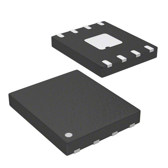
• Available in 8-DFN or 8-DFN Small Flag RoHS-compliant
package.
• Direct replacement for serial EEPROM, Flash, FeRAM
• Industrial Grade and AEC-Q100 Grade 1 and Grade 3 options
• Moisture Sensitivity MSL-3
256Kb Serial SPI MRAM
8-DFN
Small Flag 8-DFN
RoHS
Product Versions and Options
MR25H256A has been released for mass production and is recommended for all new designs.
MR25H256 remains in mass production but will be subject to eventual phase out and end of life
and is not recommended for new designs.Both versions have the same specifications.
MR25H256A Product Options
Grade
Temperature Package
Industrial
-40 to +85 C
8-DFN Small Flag
Automotive AEC-Q100 Grade 3
-40 to +85 C
8-DFN Small Flag
Automotive AEC-Q100 Grade 1
-40 to +125 C
8-DFN Small Flag
MR25H256 Product Options (Not recommended for new designs)
Grade
Temperature Package
8-DFN Small Flag
Industrial
-40 to +85 C
8-DFN
Automotive AEC-Q100 Grade 1
Copyright © 2018 Everspin Technologies
-40 to +125 C
1
8-DFN Small Flag
8-DFN
MR25H256 / MR25H256A Rev. 1.5 3/2018
�MR25H256 / MR25H256A
TABLE OF CONTENTS
OVERVIEW.............................................................................................................................................4
Figure 1 – Block Diagram............................................................................................................................................ 4
System Configuration......................................................................................................................4
Figure 2 – System Configuration.............................................................................................................................. 4
DEVICE PIN ASSIGNMENT....................................................................................................................5
Figure 3 – Pin Diagram All 8-DFN Packages......................................................................................................... 5
Table 1 – Pin Functions All 8-DFN Packages........................................................................................................ 5
SPI COMMUNICATIONS PROTOCOL....................................................................................................6
Table 2 – Command Codes........................................................................................................................................ 6
Status Register and Block Write Protection...................................................................................6
Table 3 – Status Register Bit Assignments............................................................................................................ 6
Table 4 – Block Memory Write Protection............................................................................................................. 7
Table 5 – Memory Protection Modes..................................................................................................................... 7
Read Status Register (RDSR)............................................................................................................7
Figure 4 – RDSR.............................................................................................................................................................. 7
Write Enable (WREN)........................................................................................................................8
Figure 5 – WREN............................................................................................................................................................. 8
Write Disable (WRDI)........................................................................................................................8
Figure 6 – WRDI.............................................................................................................................................................. 8
Write Status Register (WRSR)..........................................................................................................9
Figure 7 – WRSR.............................................................................................................................................................. 9
Read Data Bytes (READ)................................................................................................................ 10
Figure 8 – READ............................................................................................................................................................10
Write Data Bytes (WRITE).............................................................................................................. 11
Figure 9 – WRITE...........................................................................................................................................................11
Enter Sleep Mode (SLEEP)............................................................................................................. 12
Figure 10 – SLEEP.........................................................................................................................................................12
Copyright © 2018 Everspin Technologies
2
MR25H256 / MR25H256A Rev. 1.5 3/2018
�MR25H256 / MR25H256A
Table of Contents - Continued
Exit Sleep Mode (WAKE)................................................................................................................ 12
Figure 11 – WAKE.........................................................................................................................................................12
ELECTRICAL SPECIFICATIONS.......................................................................................................... 13
Absolute Maximum Ratings......................................................................................................... 13
Table 6 – Absolute Maximum Ratings..................................................................................................................13
Table 7 – Operating Conditions..............................................................................................................................14
Table 8 – DC Characteristics.....................................................................................................................................14
Table 9 – Power Supply Characteristics...............................................................................................................14
TIMING SPECIFICATIONS.................................................................................................................. 15
Table 10 – Capacitance..............................................................................................................................................15
Table 11 – AC Measurement Conditions.............................................................................................................15
Figure 12 – Output Load for Impedance Parameter Measurements........................................................15
Figure 13 – Output Load for All Other Parameter Measurements.............................................................15
Power-Up Timing........................................................................................................................... 16
Table 12 – Power-Up...................................................................................................................................................16
Figure 14 – Power-Up Timing.................................................................................................................................16
Synchronous Data Timing............................................................................................................. 17
Table 13 – AC Timing Parameters..........................................................................................................................17
Figure 15 – Synchronous Data Timing.................................................................................................................19
Figure 16 – HOLD Timing.........................................................................................................................................19
ORDERING INFORMATION................................................................................................................ 20
Table 14 – Ordering Part Number Decoder Table............................................................................................20
Table 15 – Ordering Part Numbers........................................................................................................................20
PACKAGE OUTLINE DRAWINGS........................................................................................................ 21
Figure 17 – 8-DFN Small Flag Package.................................................................................................................21
Figure 18 – 8-DFN Package......................................................................................................................................22
REVISION HISTORY............................................................................................................................ 23
HOW TO REACH US............................................................................................................................ 24
Copyright © 2018 Everspin Technologies
3
MR25H256 / MR25H256A Rev. 1.5 3/2018
�MR25H256 / MR25H256A
OVERVIEW
The MR25H256/MR25H256A is a serial MRAM with memory array logically organized as 32Kx8 using the four
pin interface of chip select (CS), serial input (SI), serial output (SO) and serial clock (SCK) of the serial peripheral interface (SPI) bus. Serial MRAM implements a subset of commands common to today’s SPI EEPROM
and Flash components allowing MRAM to replace these components in the same socket and interoperate
on a shared SPI bus. Serial MRAM offers superior write speed, unlimited endurance, low standby & operating
power, and more reliable data retention compared to available serial memory alternatives.
Figure 1 – Block Diagram
WP
CS
HOLD
SCK
Instruction Decode
Clock Generator
Control Logic
Write Protect
32KB
MRAM ARRAY
Instruction Register
Address Register
Counter
15
8
Data I/O Register
SI
SO
4
Nonvolatile Status
Register
System Configuration
Single or multiple devices can be connected to the bus as shown in Figure 2. Pins SCK, SO and SI are common among devices. Each device requires CS and HOLD pins to be driven separately.
Figure 2 – System Configuration
SCK
MOSI
MISO
SO
SPI
Micro Controller
SI
SCK
EVERSPIN SPI MRAM 1
CS
HOLD
SO
SI
SCK
EVERSPIN SPI MRAM 2
CS
HOLD
CS1
HOLD 1
CS2
HOLD 2
MOSI = Master Out Slave In
MISO = Master In Slave Out
Copyright © 2018 Everspin Technologies
4
MR25H256 / MR25H256A Rev. 1.5 3/2018
�MR25H256 / MR25H256A
DEVICE PIN ASSIGNMENT
Figure 3 – Pin Diagram All 8-DFN Packages
CS
1
8
VDD
SO
2
7
HOLD
WP
3
6
SCK
VSS
4
5
SI
Top View
Table 1 – Pin Functions All 8-DFN Packages
Signal Name Pin
CS
1
I/O
Input
Function
Description
Chip Select
An active low chip select for the serial MRAM. When chip select is high, the
memory is powered down to minimize standby power, inputs are ignored
and the serial output pin is Hi-Z. Multiple serial memories can share a common set of data pins by using a unique chip select for each memory.
SO
2
Output
Serial Output
The data output pin is driven during a read operation and remains Hi-Z at
all other times. SO is Hi-Z when HOLD is low. Data transitions on the data
output occur on the falling edge of SCK.
WP
3
Input
Write Protect
A low on the write protect input prevents write operations to the Status
Register.
VSS
4
Supply
Ground
SI
SCK
5
6
Input
Input
Power supply ground pin.
Serial Input
All data is input to the device through this pin. This pin is sampled on the
rising edge of SCK and ignored at other times. SI can be tied to SO to create
a single bidirectional data bus if desired.
Serial Clock
Synchronizes the operation of the MRAM. The clock can operate up to 40
MHz to shift commands, address, and data into the memory. Inputs are
captured on the rising edge of clock. Data outputs from the MRAM occur
on the falling edge of clock. The serial MRAM supports both SPI Mode 0
(CPOL=0, CPHA=0) and Mode 3 (CPOL=1, CPHA=1). In Mode 0, the clock is
normally low. In Mode 3, the clock is normally high. Memory operation is
static so the clock can be stopped at any time.
A low on the Hold pin interrupts a memory operation for another task.
When HOLD is low, the current operation is suspended. The device will
ignore transitions on the CS and SCK when HOLD is low. All transitions of
HOLD must occur while CS is low.
HOLD
7
Input
Hold
VDD
8
Supply
Power Supply
Copyright © 2018 Everspin Technologies
Power supply voltage from +2.7 to +3.6 volts.
5
MR25H256 / MR25H256A Rev. 1.5 3/2018
�MR25H256 / MR25H256A
SPI COMMUNICATIONS PROTOCOL
MR25H256/MR25H256A can be operated in either SPI Mode 0 (CPOL=0, CPHA =0) or SPI Mode 3 (CPOL=1,
CPHA=1). For both modes, inputs are captured on the rising edge of the clock and data outputs occur on
the falling edge of the clock. When not conveying data, SCK remains low for Mode 0; while in Mode 3, SCK
is high. The memory determines the mode of operation (Mode 0 or Mode 3) based upon the state of the
SCK when CS falls.
All memory transactions start when CS is brought low to the memory. The first byte is a command code. Depending upon the command, subsequent bytes of address are input. Data is either input or output. There
is only one command performed per CS active period. CS must go inactive before another command can
be accepted. To ensure proper part operation according to specifications, it is necessary to terminate each
access by raising CS at the end of a byte (a multiple of 8 clock cycles from CS dropping) to avoid partial or
aborted accesses.
Table 2 – Command Codes
Instruction
Description
Binary Code
Hex Code
Address Bytes
Data Bytes
WREN
Write Enable
0000 0110
06h
0
0
WRDI
Write Disable
0000 0100
04h
0
0
RDSR
Read Status Register
0000 0101
05h
0
1
WRSR
Write Status Register
0000 0001
01h
0
1
READ
Read Data Bytes
0000 0011
03h
2
1 to ∞
WRITE
Write Data Bytes
0000 0010
02h
2
1 to ∞
SLEEP
Enter Sleep Mode
1011 1001
B9h
0
0
WAKE
Exit Sleep Mode
1010 1011
ABh
0
0
Status Register and Block Write Protection
The status register consists of the 8 bits listed in table 2.2. Status register bits BP0 and BP1 define the memory block arrays that are protected as described in table 2.3. The Status Register Write Disable bit (SRWD)
is used in conjunction with bit 1 (WEL) and the Write Protection pin (WP) as shown in table 2.4 to enable
writes to status register bits. The fast writing speed of MR25H256/MR25H256A does not require write status
bits. The state of bits 6,5,4, and 0 can be user modified and do not affect memory operation. All bits in the
status register are pre-set from the factory to the “0” state.
Table 3 – Status Register Bit Assignments
Bit 7
Bit 6
Bit 5
Bit 4
Bit 3
Bit 2
Bit 1
Bit 0
SRWD
Don’t Care
Don’t Care
Don’t Care
BP1
BP0
WEL
Don’t Care
Copyright © 2018 Everspin Technologies
6
MR25H256 / MR25H256A Rev. 1.5 3/2018
�MR25H256 / MR25H256A
Table 4 – Block Memory Write Protection
Status Register
BP1
BP0
0
0
0
1
1
0
1
1
Memory Contents
Protected Area
None
Upper Quarter
Upper Half
All
Unprotected Area
All Memory
Lower Three-Quarters
Lower Half
None
Table 5 – Memory Protection Modes
WEL
0
1
1
1
SRWD
WP
Protected Blocks
Unprotected Blocks
X
0
1
1
X
X
Low
High
Protected
Protected
Protected
Protected
Protected
Writable
Writable
Writable
Status
Register
Protected
Writable
Protected
Writable
When WEL is reset to 0, writes to all blocks and the status register are protected. When WEL is set to 1, BP0
and BP1 determine which memory blocks are protected. While SRWD is reset to 0 and WEL is set to 1, status
register bits BP0 and BP1 can be modified. Once SRWD is set to 1, WP must be high to modify SRWD, BP0 and
BP1.
Read Status Register (RDSR)
The Read Status Register (RDSR) command allows the Status Register to be read. The Status Register can be
read at any time to check the status of write enable latch bit, status register write protect bit, and block write
protect bits. For MR25H256/MR25H256A, the write in progress bit (bit 0) is not written by the memory because there is no write delay. The RDSR command is entered by driving CS low, sending the command code,
and then driving CS high.
Figure 4 – RDSR
CS
0
1
2
3
4
5
6
7
0
1
2
3
4
5
6
7
SCK
SI
Mode 3
Mode 0
0
0
0
0
0
1
0
1
MSB
Status Register Out
SO
High Impedance
7
6
5
4
3
2
1
0
High Z
MSB
Copyright © 2018 Everspin Technologies
7
MR25H256 / MR25H256A Rev. 1.5 3/2018
�MR25H256 / MR25H256A
Write Enable (WREN)
The Write Enable (WREN) command sets the Write Enable Latch (WEL) bit in the status register to 1. The WEL
bit must be set prior to writing in the status register or the memory. The WREN command is entered by driving CS low, sending the command code, and then driving CS high.
Figure 5 – WREN
CS
Mode 3
SCK
0
1
2
3
4
5
6
Mode 3
7
Mode 0
Mode 0
Instruction (06h)
SI
0
0
0
0
0
1
1
0
High Impedance
SO
Write Disable (WRDI)
The Write Disable (WRDI) command resets the WEL bit in the status register to 0. This prevents writes to
status register or memory. The WRDI command is entered by driving CS low, sending the command code,
and then driving CS high.
The WEL bit is reset to 0 on power-up or completion of WRDI.
Figure 6 – WRDI
CS
Mode 3
SCK
0
1
2
3
4
5
6
7
Mode 3
Mode 0
Mode 0
Instruction (04h)
SI
0
SO
Copyright © 2018 Everspin Technologies
0
0
0
0
1
0
0
High Impedance
8
MR25H256 / MR25H256A Rev. 1.5 3/2018
�MR25H256 / MR25H256A
Write Status Register (WRSR)
The Write Status Register (WRSR) command allows new values to be written to the Status Register. The
WRSR command is not executed unless the Write Enable Latch (WEL) has been set to 1 by executing a WREN
command while pin WP and bit SRWD correspond to values that make the status register writable as seen in
table 2.4. Status Register bits are non-volatile with the exception of the WEL which is reset to 0 upon power
cycling.
The WRSR command is entered by driving CS low, sending the command code and status register write data
byte, and then driving CS high.
Figure 7 – WRSR
CS
0
1
2
3
4
5
6
7
8
9
10
11
12
13
14
15 Mode 3
SCK
Mode 0
Instruction (01h)
SI
0
0
0
0
0
0
Status Register In
0
1
7
6
5
4
3
2
1
0
MSB
SO
Copyright © 2018 Everspin Technologies
High Impedance
9
MR25H256 / MR25H256A Rev. 1.5 3/2018
�MR25H256 / MR25H256A
Read Data Bytes (READ)
The Read Data Bytes (READ) command allows data bytes to be read starting at an address specified by the
16-bit address. Only address bits 0-14 are decoded by the memory. The data bytes are read out sequentially
from memory until the read operation is terminated by bringing CS high The entire memory can be read in a
single command. The address counter will roll over to 0000h when the address reaches the top of memory.
The READ command is entered by driving CS low and sending the command code. The memory drives the
read data bytes on the SO pin. Reads continue as long as the memory is clocked. The command is terminated by bring CS high.
Figure 8 – READ
CS
0
1
2
3
4
5
6
7
8
9
10
20
21
22
23
24
25
26
27
28
29
30
31
SCK
Instruction (03h)
SI
0
0
0
0
0
0
16-Bit Address
1
1
X
14
13
3
2
1
0
MSB
SO
Data Out 1
High Impedance
7
6
5
4
3
Data Out 2
2
1
0
7
MSB
Copyright © 2018 Everspin Technologies
10
MR25H256 / MR25H256A Rev. 1.5 3/2018
�MR25H256 / MR25H256A
Write Data Bytes (WRITE)
The Write Data Bytes (WRITE) command allows data bytes to be written starting at an address specified by
the 16-bit address. Only address bits 0-14 are decoded by the memory. The data bytes are written sequentially in memory until the write operation is terminated by bringing CS high. The entire memory can be
written in a single command. The address counter will roll over to 0000h when the address reaches the top
of memory.
Unlike EEPROM or Flash Memory, MRAM can write data bytes continuously at its maximum rated clock
speed without write delays or data polling. Back to back WRITE commands to any random location in memory can be executed without write delay. MRAM is a random access memory rather than a page, sector, or
block organized memory making it ideal for both program and data storage.
The WRITE command is entered by driving CS low, sending the command code, and then sequential write
data bytes. Writes continue as long as the memory is clocked. The command is terminated by bringing CS
high.
Figure 9 – WRITE
CS
0
1
2
3
4
5
6
7
8
9
20
10
21
22
23
24
25
26
27
28
29
30
31
SCK
Instruction (02h)
SI
0
0
0
0
0
16-Bit Address
0
1
0
14
X
13
3
2
1
0
MSB
7
6
5
4
3
2
1
0
MSB
High Impedance
SO
CS
32
33
34
35
36
37
38
39
40
41
42
43
44
45
46
Mode 3
47
SCK
Mode 0
Data Byte 2
SI
7
6
5
4
3
Data Byte 3
2
1
0
7
6
5
4
MSB
3
Data Byte N
2
1
0
7
6
5
4
3
2
1
0
MSB
High Impedance
SO
Copyright © 2018 Everspin Technologies
11
MR25H256 / MR25H256A Rev. 1.5 3/2018
�MR25H256 / MR25H256A
Enter Sleep Mode (SLEEP)
The Enter Sleep Mode (SLEEP) command turns off all MRAM power regulators in order to reduce the overall
chip standby power to 3 μA typical. The SLEEP command is entered by driving CS low, sending the command code, and then driving CS high. The standby current is achieved after time, tDP. If power is removed
when the part is in sleep mode, upon power restoration, the part enters normal standby. The only valid
command following SLEEP mode entry is a WAKE command.
Figure 10 – SLEEP
CS
t DP
0
1
2
3
4
5
6
Mode 3
7
SCK
Mode 0
Instruction (B9h)
SI
1
0
1
1
1
0
0
1
Active Current
Standby Current
Sleep Mode Current
SO
Exit Sleep Mode (WAKE)
The Exit Sleep Mode (WAKE) command turns on internal MRAM power regulators to allow normal operation.
The WAKE command is entered by driving CS low, sending the command code, and then driving CS high.
The memory returns to standby mode after tRDP. The CS pin must remain high until the tRDP period is over.
Figure 11 – WAKE
CS
t RDP
0
1
2
3
4
5
6
7
SCK
Mode 3
Mode 0
Instruction (ABh)
SI
1
0
1
0
1
0
1
Sleep Mode Current
1
Standby Current
SO
Copyright © 2018 Everspin Technologies
12
MR25H256 / MR25H256A Rev. 1.5 3/2018
�MR25H256 / MR25H256A
ELECTRICAL SPECIFICATIONS
Absolute Maximum Ratings
This device contains circuitry to protect the inputs against damage caused by high static voltages or electric
fields; however, it is advised that normal precautions be taken to avoid application of any voltage greater
than maximum rated voltages to these high-impedance (Hi-Z) circuits.
The device also contains protection against external magnetic fields. Precautions should be taken to avoid
application of any magnetic field more intense than the field intensity specified in the maximum ratings.
Table 6 – Absolute Maximum Ratings
Symbol
Parameter
Conditions
VDD
Supply voltage 2
VIN
Value 1
Unit
All
-0.5 to 4.0
V
Voltage on any pin 2
All
-0.5 to VDD + 0.5
V
IOUT
Output current per pin
All
±20
mA
PD
Package power dissipation 3
All
0.600
W
Industrial
-45 to 95
°C
AEC-Q100 Grade 3
-45 to 95
°C
AEC-Q100 Grade 1
-45 to 135
°C
TBIAS
Temperature under bias
Tstg
Storage Temperature
All
-55 to 150
°C
TLead
Lead temperature during solder (3
minute max)
All
260
°C
Hmax_write
Maximum magnetic field (Write)
During Write
12,000
A/m
Hmax_read
Maximum magnetic field (Read or
Standby)
During Read or
Standby
12,000
A/m
Notes:
1. Permanent device damage may occur if absolute maximum ratings are exceeded. Functional operation should be restricted to recommended operating conditions. Exposure to excessive voltages or
magnetic fields could affect device reliability.
2. All voltages are referenced to VSS. The DC value of VIN must not exceed actual applied VDD by more
than 0.5V. The AC value of VIN must not exceed applied VDD by more than 2V for 10ns with IIN limited
to less than 20mA.
3. Power dissipation capability depends on package characteristics and use environment.
Copyright © 2018 Everspin Technologies
13
MR25H256 / MR25H256A Rev. 1.5 3/2018
�MR25H256 / MR25H256A
Table 7 – Operating Conditions
Symbol
VDD
Parameter
Power supply voltage
Grade
Min
Typical
Max
Unit
Industrial
2.7
-
3.6
V
AEC-Q100 Grade 3
2.7
-
3.6
V
AEC-Q100 Grade1
3.0
-
3.6
V
VIH
Input high voltage
All
2.2
-
VDD + 0.3
V
VIL
Input low voltage
All
-0.5
-
0.8
V
Industrial
-40
-
85
°C
-40
-
85
°C
-40
-
125
°C
TA
Temperature under bias AEC-Q100 Grade 3
AEC-Q100 Grade 1 1
1. AEC-Q100 Grade 1 temperature profile assumes 10 percent duty cycle at maximum temperature (2 years
out of 20-year life.)
Table 8 – DC Characteristics
Symbol Parameter
Conditions
Min
Typical
Max
Unit
ILI
Input leakage current
All
-
-
±1
μA
ILO
Output leakage current
All
-
-
±1
μA
IOL = +4 mA
-
-
0.4
V
IOL = +100 μA
-
-
VSS + 0.2v
V
2.4
-
-
V
VDD - 0.2
-
-
V
VOL
VOH
Output low voltage
Output high voltage
IOH = -4 mA
IOH = -100 μA
Table 9 – Power Supply Characteristics
Symbol Parameter
IDDR
Active Read Current
IDDW
Active Write Current
Conditions
Typical
Max
Unit
@ 1 MHz
2.5
3
mA
@ 40 MHz
6
10
mA
@ 1 MHz
8
13
mA
@ 40 MHz
23
27
mA
ISB
Standby Current
CS High 1
90
115
μA
IZZ
Standby Sleep Mode Current
CS High
7
30
μA
1. ISB current is specified with CS high and the SPI bus inactive.
Copyright © 2018 Everspin Technologies
14
MR25H256 / MR25H256A Rev. 1.5 3/2018
�MR25H256 / MR25H256A
TIMING SPECIFICATIONS
Table 10 – Capacitance
Symbol
Parameter
Typical
Max 1
Unit
CIn
Control input capacitance
-
6
pF
CI/O
Input/Output capacitance
-
8
pF
1. ƒ = 1.0 MHz, dV = 3.0 V, TA = 25 °C, periodically sampled rather than 100% tested.
Table 11 – AC Measurement Conditions
Parameter
Value
Unit
Logic input timing measurement reference level
1.5
V
Logic output timing measurement reference level
1.5
V
0 or 3.0
V
2
ns
Logic input pulse levels
Input rise/fall time
Output load for low and high impedance parameters
See Figure 4.1
Output load for all other timing parameters
See Figure 4.2
Figure 12 – Output Load for Impedance Parameter Measurements
ZD= 50 Ω
Output
RL = 50 Ω
VL = 1.5 V
Figure 13 – Output Load for All Other Parameter Measurements
3.3 V
590 Ω
Output
30 pF
435 Ω
Copyright © 2018 Everspin Technologies
15
MR25H256 / MR25H256A Rev. 1.5 3/2018
�MR25H256 / MR25H256A
Power-Up Timing
The MR25H256/MR25H256A is not accessible for a start-up time tPU = 400 μs after power up. Users must
wait this time from the time when VDD (min) is reached until the first CS low to allow internal voltage references to become stable. The CS signal should be pulled up to VDD so that the signal tracks the power supply
during power-up sequence.
Table 12 – Power-Up
Symbol
Parameter
Min
Typical
Max
Unit
VWI
Write Inhibit Voltage
2.2
-
2.7
V
t
Startup Time
400
-
-
μs
PU
Figure 14 – Power-Up Timing
VDD
VDD(max)
Chip Selection not allowed
VDD(min)
Reset state
of the
device
t PU
Normal Operation
VWI
Time
Copyright © 2018 Everspin Technologies
16
MR25H256 / MR25H256A Rev. 1.5 3/2018
�MR25H256 / MR25H256A
Synchronous Data Timing
Table 13 – AC Timing Parameters
Over the Operating Temperature Range and CL = 30 pF
Symbol
f
Parameter
Min
Max
Unit
SCK
SCK Clock Frequency
0
40
MHz
t
RI
Input Rise Time
-
50
ns
t
RF
Input Fall Time
-
50
ns
t
WH
SCK High Time
11
-
ns
t
SCK Low Time
11
-
ns
WL
Synchronous Data Timing (See “Figure 15 – Synchronous Data Timing” on page 19
t
CS
CS High Time
40
-
ns
t
CSS
CS Setup Time
10
-
ns
t
CSH
CS Hold Time
10
-
ns
t
SU
Data In Setup Time
5
-
ns
t
Data In Hold Time
5
-
ns
VDD = 2.7 to 3.6v.
0
10
ns
VDD = 3.0 to 3.6v.
0
9
ns
VDD = 2.7 to 3.6v.
0
10
ns
VDD = 3.0 to 3.6v.
0
9
ns
VDD = 3.0 to 3.6v.
0
10
ns
H
Industrial Grade
t
V
Output Valid
AEC Q-100 Grade 3
AEC Q-100 Grade 1
Table continues next page.
Copyright © 2018 Everspin Technologies
17
MR25H256 / MR25H256A Rev. 1.5 3/2018
�MR25H256 / MR25H256A
AC Timing Parameters (Continued)
Symbol
Parameter
Min
Max
Unit
Output Hold Time
0
-
ns
HD
HOLD Setup Time
10
-
ns
t
CD
HOLD Hold Time
10
-
ns
t
LZ
HOLD to Output Low Impedance
-
20
ns
t
HZ
HOLD to Output High Impedance
-
20
ns
t
HO
HOLD Timing
t
Other Timing Specifications (See “Figure 16 – HOLD Timing” on page 19)
t
WPS
WP Setup To CS Low
5
-
ns
t
WPH
WP Hold From CS High
5
-
ns
t
DP
Sleep Mode Entry Time
3
-
μs
RDP
Sleep Mode Exit Time
400
-
μs
t
Output Disable Time
12
-
ns
t
DIS
Copyright © 2018 Everspin Technologies
18
MR25H256 / MR25H256A Rev. 1.5 3/2018
�MR25H256 / MR25H256A
Figure 15 – Synchronous Data Timing
Figure 16 – HOLD Timing
CS
tCD
tCD
SCK
tHD
tHD
HOLD
tHZ
tLZ
SO
Copyright © 2018 Everspin Technologies
19
MR25H256 / MR25H256A Rev. 1.5 3/2018
�MR25H256 / MR25H256A
ORDERING INFORMATION
Table 14 – Ordering Part Number Decoder Table
Table 15 – Ordering Part Numbers
Grade
Temperature Package
Industrial
-40 to +85 C
8-DFN Small Flag
AEC-Q100 Grade 3 -40 to +85 C
8-DFN Small Flag
AEC-Q100 Grade 1 -40 to +125 C
8-DFN Small Flag
Industrial
-40 to +85 C
8-DFN Small Flag
Industrial
-40 to +85 C
8-DFN
AEC-Q100 Grade 1 -40 to +125 C
AEC-Q100 Grade 1 -40 to +125 C
8-DFN Small Flag
8-DFN
Shipping Container
Trays
Tape and Reel
Trays
Tape and Reel
Trays
Tape and Reel
Trays
Order Part Number
MR25H256ACDF
MR25H256ACDFR
MR25H256APDF
MR25H256APDFR
MR25H256AMDF
MR25H256AMDFR
MR25H256CDF 1
Tape and Reel
MR25H256CDFR 1
Trays
MR25H256CDC 1
Tape and Reel
MR25H256CDCR 1
Trays
MR25H256MDF 1
Tape and Reel
MR25H256MDFR 1
Trays
MR25H256MDC 1
Tape and Reel
MR25H256MDCR 1
Note:
1. Not recommended for new designs.
Copyright © 2018 Everspin Technologies
20
MR25H256 / MR25H256A Rev. 1.5 3/2018
�MR25H256 / MR25H256A
PACKAGE OUTLINE DRAWINGS
Figure 17 – 8-DFN Small Flag Package
A
2X
Exposed metal Pad. Do not connect anything except VSS
0.10 C
8
5
2X
J
B
I
G
L
H
M
Pin 1 Index
C
Detail A
D
1
4
F
0.10 C
K
F
E
Detail A
A
B
C
D
E
F
G
H
I
J
K
L
M
Max
5.10
6.10
0.90
-
0.45
0.05
1.54
0.70
2.10
2.10
0.210
-
-
Nominal
5.00
6.00
0.85
0.40
-
1.40
0.60
2.00
2.00
0.200
C0.45
R0.20
Min
4.90
5.90
0.80
0.35
0.00
1.26
0.50
1.90
1.90
0.190
-
-
Dimension
1.27
BSC
-
NOTE:
1. All dimensions are in mm. Angles in degrees.
2. Coplanarity applies to the exposed pad as well as the terminals. Coplanarity shall be
within 0.08 mm.
3. Refer to JEDEC MO-229-E
Copyright © 2018 Everspin Technologies
21
MR25H256 / MR25H256A Rev. 1.5 3/2018
�MR25H256 / MR25H256A
Figure 18 – 8-DFN Package
Not Recommended for New Designs
Exposed metal Pad. Do not
connect anything except VSS
8
A
5
DAP Size
4.4 x 4.4
J
B
I
L
G
H
M
Pin 1 Index
C
Detail A
D
K
N
E
Detail A
A
B
C
D
E
Max.
5.10
6.10
1.00
1.27
0.45
Min.
4.90
5.90
0.90
BSC
0.35
Dimension
1
4
F
F
G
H
I
J
K
0.05
0.35
0.70
4.20
4.20
0.261
0.00
Ref.
0.50
4.00
4.00
0.195
L
C0.35
M
R0.20
N
0.05
0.00
NOTE:
1. All dimensions are in mm. Angles in degrees.
2. Coplanarity applies to the exposed pad as well as the terminals. Coplanarity shall be
within 0.08 mm.
3. Warpage shall not exceed 0.10 mm.
4. Refer to JEDEC MO-229-E
Copyright © 2018 Everspin Technologies
22
MR25H256 / MR25H256A Rev. 1.5 3/2018
�MR25H256 / MR25H256A
REVISION HISTORY
Revision
Date
0.1
June 1, 2015
0.2
September 29,
2015
0.3
Description of Change
First Draft
Added Grade 3 parameters to Table 4.4 and reformatted the table.
November 2, 2015 Revised Part Number Decoder Table.
1.0
October 1, 2016
Production release. Removed all Preliminary status statements and
indications. Added nominal values to DFN package outline dimensions
table.
1.1
October 12, 2016
Combined with MR25H256 to make single data sheet for both product
families.
1.2
December 13,
2016
Revised product name in header.
1.3
December 20,
2016
Minor Revisions. 8-DFN package option will remain.
1.4
February 1, 2017
t
t
Added HO and V relationship to Synchronous Data Timing
1.5
March 23, 2018
Updated the Contact Us table
Copyright © 2018 Everspin Technologies
23
MR25H256 / MR25H256A Rev. 1.5 3/2018
�MR25H256 / MR25H256A
HOW TO REACH US
Everspin Technologies, Inc.
How to Reach Us:
Home Page:
www.everspin.com
World Wide Information Request
WW Headquarters - Chandler, AZ
5670 W. Chandler Blvd., Suite 100
Chandler, Arizona 85226
Tel: +1-877-480-MRAM (6726)
Local Tel: +1-480-347-1111
Fax: +1-480-347-1175
support@everspin.com
orders@everspin.com
sales@everspin.com
Europe, Middle East and Africa
Everspin Europe Support
support.europe@everspin.com
Japan
Everspin Japan Support
support.japan@everspin.com
Asia Pacific
Everspin Asia Support
support.asia@everspin.com
Information in this document is provided solely to enable system and software implementers to use Everspin Technologies products. There are no
express or implied licenses granted hereunder to design or fabricate any
integrated circuit or circuits based on the information in this document.
Everspin Technologies reserves the right to make changes without further
notice to any products herein. Everspin makes no warranty, representation or guarantee regarding the suitability of its products for any particular purpose, nor does Everspin Technologies assume any liability arising
out of the application or use of any product or circuit, and specifically
disclaims any and all liability, including without limitation consequential
or incidental damages. “Typical” parameters, which may be provided in
Everspin Technologies data sheets and/or specifications can and do vary
in different applications and actual performance may vary over time. All
operating parameters including “Typicals” must be validated for each customer application by customer’s technical experts. Everspin Technologies
does not convey any license under its patent rights nor the rights of others. Everspin Technologies products are not designed, intended, or authorized for use as components in systems intended for surgical implant
into the body, or other applications intended to support or sustain life, or
for any other application in which the failure of the Everspin Technologies
product could create a situation where personal injury or death may occur. Should Buyer purchase or use Everspin Technologies products for any
such unintended or unauthorized application, Buyer shall indemnify and
hold Everspin Technologies and its officers, employees, subsidiaries, affiliates, and distributors harmless against all claims, costs, damages, and expenses, and reasonable attorney fees arising out of, directly or indirectly,
any claim of personal injury or death associated with such unintended or
unauthorized use, even if such claim alleges that Everspin Technologies
was negligent regarding the design or manufacture of the part. Everspin™
and the Everspin logo are trademarks of Everspin Technologies, Inc. All
other product or service names are the property of their respective owners.
Copyright © 2018 Everspin Technologies, Inc.
Filename:
EST02896MR25H256-MR25H256ADatasheet_Rev1.5032318
Copyright © 2018 Everspin Technologies
24
MR25H256 / MR25H256A Rev. 1.5 3/2018
�


 工商网监
湘ICP备2023018690号
工商网监
湘ICP备2023018690号
