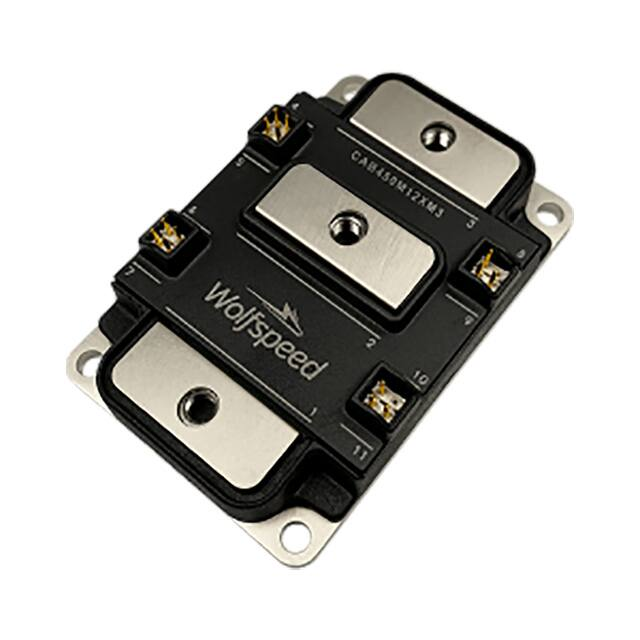
CAB450M12XM3
1200V, 450A All-Silicon Carbide
Conduction Optimized, Half-Bridge Module
Technical Features
5
VDS
1200 V
IDS
450 A
4
3
2
Package
80 x 53 x 19 mm
D
•
•
•
•
High Power Density Footprint
High Junction Temperature (175 °C) Operation
Low Inductance (6.7 nH) Design
Implements Conduction Optimized Third
Generation SiC MOSFET Technology
• Silicon Nitride Insulator and Copper Baseplate
V+
V+
G1
K1
C
Mid
Applications
•
•
•
•
NTC2
Motor & Traction Drives
Vehicle Fast Chargers
Uninterruptable Power Supplies
Smart-Grid / Grid-Tied Distributed Generation
G2
NTC
K2
NTC1
VB
System Benefits
• Terminal layout allows for direct bus bar connection without bends or bushings enabling a simple,
low inductance design.
• Isolated integrated temperature sensing enables high-level temperature protection.
• Dedicated drain Kelvin pin enables direct voltage sensing for gate driver overcurrentTitle
protection.
A
Size
Document Number
Custom
Key Parameters (TC = 25˚C unless otherwise specified)
Drain-Source Voltage
VGS max
Gate-Source Voltage, Maximum Value
-4
+19
VGS op
Gate-Source Voltage, Recommended
Op. Value
-4
+15
Static
450
VGS = 15 V, TC = 25 ˚C, TVJ ≤ 175 ˚C Fig. 20
ISD
DC Source-Drain Current
Max.
Note
450
225
ISD (pulsed) Maximum Pulsed Source-Drain Current
900
-40
AC frequency ≥ 1Hz.
Note 1
VGS = 15 V, TC = 90 ˚C, TVJ ≤ 175 ˚C Note 2
900
Note 1
Note 2
V
409
DC Source-Drain Current (Body Diode)
Maximum Virtual Junction
Temperature under Switching
Conditions
Test Conditions
1200
IDS (pulsed) Maximum Pulsed Drain-Source Current
TVJ op
Unit
2
VDS max
DC Continuous Drain Current
Typ.
Sheet
3
Parameter
IDS
Min.
4
Symbol
ISD BD
1
Thursday, April 11, 2019
Date:
5
175
A
VGS = 15 V, TC = 25 ˚C, TVJ ≤ 175 ˚C
VGS = - 4 V, TC = 25 ˚C, TVJ ≤ 175 ˚C
tPmax limited by Tjmax
VGS = 15 V, TC = 25 ˚C
°C
If MOSFET body diode is not used, VGS max = -8/+19 V
Assumes RTH JC = 0.11°C/W and RDS(on) = 4.6 mΩ. Calculate PD = (TVJ – TC) / RTH JC. Calculate ID_MAX = √(PD / RDS(on))
Rev. A, 2019-06-01
CAB450M12XM3
4600 Silicon Dr., Durham, NC 27703
Copyright ©2019 Cree, Inc. All rights reserved. The information in this document is subject to change without notice. Cree®, the Cree logo, Wolfspeed®, and the Wolfspeed logo
are registered trademarks of Cree, Inc.
�MOSFET Characteristics (Per Position) (TC = 25˚C unless otherwise specified)
Symbol
Parameter
Min.
V(BR)DSS
Drain-Source Breakdown Voltage
1200
VGS(th)
Gate Threshold Voltage
IDSS
Zero Gate Voltage Drain Current
IGSS
RDS(on)
1.8
Typ.
2.5
200
Gate-Source Leakage Current
0.05
1.3
Drain-Source On-State Resistance (Devices
Only)
2.6
3.7
4.6
355
EOn
Turn-On Switching Energy, TJ = 25 °C
TJ = 125 °C
TJ = 175 °C
11.0
11.7
13.0
Turn-Off Switching Energy, TJ = 25 °C
TJ = 125 °C
TJ = 175 °C
10.1
11.3
12.1
Internal Gate Resistance
2.5
Ciss
Input Capacitance
38.0
Coss
Output Capacitance
1.5
Crss
Reverse Transfer Capacitance
90
QGS
Gate to Source Charge
355
QGD
Gate to Drain Charge
500
QG
Total Gate Charge
1330
FET Thermal Resistance, Junction to Case
0.11
Rth JC
V
Test Conditions
Note
VGS = 0 V, ID = 200 μA
VDS = VGS, ID = 132 mA
VDS = VGS, ID = 132 mA, TJ = 175 °C
5
Transconductance
RG(int)
3.6
Unit
2.0
gfs
EOff
Max.
μA
mΩ
S
360
mJ
Ω
nF
pF
nC
0.13
VGS = 0 V, VDS = 1200 V
VGS = 15 V, VDS = 0 V
VGS = 15 V, ID = 450 A
VGS = 15 V, ID = 450 A, TJ = 175 °C
VDS= 20 V, IDS= 450 A
VDS= 20 V, IDS= 450 A, TJ = 175 °C
VDS = 600 V,
ID = 450A,
VGS = -4 V/15 V,
RG(ext) = 0.0 Ω,
L= 13.6 μH
VGS = 0 V, VDS = 800 V,
VAC = 25 mV, f = 100 kHz
Fig. 2
Fig. 3
Fig. 4
Fig. 11
Fig. 13
Fig. 9
VDS = 800 V, VGS = -4 V/15 V
ID = 450 A
Per IEC60747-8-4 pg 21
°C/W
Fig. 17
Body Diode Characteristics (Per Position) (TC = 25˚C unless otherwise specified)
Symbol Parameter
2
Min.
Typ.
4.7
Max.
Unit
VSD
Body Diode Forward Voltage
trr
Reverse Recovery Time
52
ns
Qrr
Reverse Recovery Charge
6.6
Irr
Peak Reverse Recovery Current
195
μC
Err
Reverse Recovery Energy TJ = 25 °C
TJ = 125 °C
TJ = 175 °C
0.2
1.1
1.9
4.2
V
A
mJ
Test Conditions
VGS = -4 V, ISD = 450 A
VGS = -4 V, ISD = 450 A, TJ = 175 °C
Note
Fig. 7
VGS = -4 V, ISD = 450 A, VR = 600 V
di/dt = 8 A/ns, TJ = 175 °C
VDS = 600 V, ID = 450A,
VGS = -4 V/15 V, RG(ext) = 0.0 Ω,
L= 13.6 μH
Rev. A, 2019-06-01
CAB450M12XM3
4600 Silicon Dr., Durham, NC 27703
Copyright ©2019 Cree, Inc. All rights reserved. The information in this document is subject to change without notice. Cree®, the Cree logo, Wolfspeed®, and the Wolfspeed logo
are registered trademarks of Cree, Inc.
Fig. 14
�Temperature Sensor (NTC) Characteristics
Symbol Parameter
R25
∆R/R
P25
Min.
Typ.
Rated Resistance
Max.
4.7
Unit
kΩ
Tolerance of R25
±1
%
Maximum Power Dissipation
50
mW
Test Conditions
TNTC = 25 °C
Steinhart-Hart Modified Coefficients for R/T Computation:
A
B
C
D
TNTC < 25 °C
3.3540E-03
3.0013E-04
5.0852E-06
2.1877E-07
TNTC ≥ 25 °C
3.3540E-03
3.0013E-04
5.0852E-06
2.1877E-07
Module Physical Characteristics
Symbol Parameter
Min.
R3-1
Package Resistance, M1
0.72
R1-2
Package Resistance, M2
0.63
LStray
Stray Inductance
6.7
TC
Case Temperature
W
Weight
MS
Mounting Torque
Visol
Case Isolation Voltage
4.0
CTI
Comparative Tracking Index
600
Clearance Distance
-40
Note13
Note24
Unit
mΩ
nH
125
Test Conditions
TC = 125 °C, Note13
TC = 125 °C, Note 3
Between Terminals 2 and 3
°C
g
2.0
3.0
4.0
2.0
4.0
5.0
N-m
kV
Baseplate, M4 bolts
Power Terminals, M5 bolts
AC, 50 Hz, 1 min
12.5
From 2 to 3, Note24
11.5
From 1 to Baseplate, Note 4
5.7
From 2 to 5, Note 4
14.7
Creepage Distance
Max.
175
13.7
3
Typ.
mm
From 5 to Baseplate, Note 4
From 2 to 3, Note 4
14.0
From 1 to Baseplate, Note 4
14.7
From 2 to 5, Note 4
14.3
From 5 to Baseplate, Note 4
Total Effective Resistance (Per Switch Position) = MOSFET RDS(on) + Switch Position Package Resistance.
Numbers reference the connections from the Schematic and Package Dimensions sections of this document.
Rev. A, 2019-06-01
CAB450M12XM3
4600 Silicon Dr., Durham, NC 27703
Copyright ©2019 Cree, Inc. All rights reserved. The information in this document is subject to change without notice. Cree®, the Cree logo, Wolfspeed®, and the Wolfspeed logo
are registered trademarks of Cree, Inc.
�Typical Performance
900
2.0
Drain-Source Current, IDS (A)
800
700
600
Normalized On-resistance (p.u.)
Conditions:
tp < 300 μs
VGS = 15 V
25 °C
-40 °C
500
400
100 °C
125 °C
150 °C
175 °C
300
200
100
0
0.0
1.0
2.0
3.0
4.0
5.0
1.8
150 °C
1.2
0.8
700
600
0
100
200
300
400
500
600
700
800
900
Conditions:
tp < 300 μs
VDS = 20 V
175 °C
150 °C
125 °C
100 °C
400
1.0
0.8
300
0.6
200
0.4
0.2
25 °C
0 °C
-25 °C
-40 °C
100
-50
0
50
100
150
0
200
Virtual Junction Temperature, TVJ (°C)
Source-Drain Current, ISD (A)
800
700
900
Conditions:
tp < 300 μs
VGS = 15 V
800
700
600
4.0
Conditions:
tp < 300 μs
VGS = 0.0 V
500
25 °C
-40 °C
400
6.0
8.0
400
300
25 °C
0 °C
-25 °C
-40 °C
300
100 °C
125 °C
150 °C
175 °C
200
100
0.0
1.0
2.0
10.0
175 °C
150 °C
125 °C
100 °C
600
500
0
2.0
Figure 4. Transfer Characteristic for Various Junction
Temperatures
Source-Drain Current, ISD (A)
900
0.0
Gate-Source Voltage, VGS (V)
Figure 3. Normalized On-State Resistance vs.
Juction Temperature
200
100
3.0
4.0
5.0
6.0
Source-Drain Voltage, VSD (V)
Figure 5. 3rd Quadrant Characteristic vs. Junction Temperatures at VGS = 15
V
4
25 °C
500
1.2
0.0
-40 °C
1.0
Drain-Source Current, IDS (A)
Normalized On-resistance (p.u.)
1.4
100 °C
Figure 2. Normalized On-State Resistance vs. Drain Current for Various
Juction Temperatures
Conditions:
tp < 300 μs
VGS = 15 V
ID = 450 A
1.6
125 °C
1.4
Drain-Source Current, IDS (A)
Figure 1. Output Characteristics for Various Junction
Temperatures
1.8
175 °C
1.6
Drain-Source Voltage, VDS (V)
2.0
Conditions:
tp < 300 μs
VGS = 15 V
0
0.0
1.0
2.0
3.0
4.0
5.0
6.0
Source-Drain Voltage, VSD (V)
Figure 6. 3rd Quadrant Characteristic vs. Junction Temperatures at VGS = 0
V (Body Diode)
Rev. A, 2019-06-01
CAB450M12XM3
4600 Silicon Dr., Durham, NC 27703
Copyright ©2019 Cree, Inc. All rights reserved. The information in this document is subject to change without notice. Cree®, the Cree logo, Wolfspeed®, and the Wolfspeed logo
are registered trademarks of Cree, Inc.
�Typical Performance
900
1,000.00
Conditions:
tp < 300 μs
VGS = - 4.0 V
700
600
175 °C
150 °C
125 °C
100 °C
500
400
300
200
0.0
1.0
2.0
3.0
4.0
5.0
0.10
6.0
0.01
7.0
1,000.00
Coss
400
600
2.5
2.0
1.5
1.0
0.5
800
1,000
1,200
-50
0
100
150
200
Figure 10. Threshold Voltage vs. Junction Temperature
60
80
Conditions:
TVJ = 25 °C
VDS = 600 V
RG(ext) = 0.0 Ω
VGS = -4/+15 V
L = 13.6 µH
40
EOn + EOff
30
EOff
EOn
20
10
ERR
0
200
400
600
800
Drain-Source Current, IDS (A)
Figure 11. Switching Energy vs. Drain Current
(VDS = 600 V)
Conditions:
TVJ = 25 °C
VDS = 800 V
RG(ext) = 0.0 Ω
VGS = -4/+15 V
L = 13.6 µH
70
Switching Energy (mJ)
50
Switching Energy (mJ)
50
Junction Temperature, TJ (°C)
Figure 9. Typical Capacitances vs. Drain to Source Voltage
(0 - 1200V)
5
200
Conditions:
VGS = VDS
IDS = 132 mA
Drain-Source Voltage, VDS (V)
0
150
3.0
0.0
200
100
3.5
Crss
0
50
4.0
Thresold Voltage, Vth (V)
Capacitance (nF)
Ciss
10.00
0.01
0
Figure 8. Typical Capacitances vs. Drain to Source Voltage
(0 - 200V)
TJ = 25 °C
VAC = 25 mV
f = 100 kHz
0.10
Crss
Drain-Source Voltage, VDS (V)
Figure 7. 3rd Quadrant Characteristic vs. Junction Temperatures at
VGS = - 4 V (Body Diode)
1.00
Coss
1.00
Source-Drain Voltage, VSD (V)
100.00
Ciss
10.00
25 °C
0 °C
-25 °C
-40 °C
100
0
TJ = 25 °C
VAC = 25 mV
f = 100 kHz
100.00
Capacitance (nF)
Source-Drain Current, ISD (A)
800
1000
60
50
EOn + EOff
40
EOff
30
EOn
20
10
0
ERR
0
200
400
600
800
Drain-Source Current, IDS (A)
Figure 12. Switching Energy vs. Drain Current
(VDS = 800 V)
Rev. A, 2019-06-01
CAB450M12XM3
4600 Silicon Dr., Durham, NC 27703
Copyright ©2019 Cree, Inc. All rights reserved. The information in this document is subject to change without notice. Cree®, the Cree logo, Wolfspeed®, and the Wolfspeed logo
are registered trademarks of Cree, Inc.
1000
�Typical Performance
25
Switching Energy (mJ)
2.5
Conditions:
IDS = 450 A, VDD =600 V
RG(ext) = 0.0 Ω, VGS = -4/+15 V
L = 13.6 µH
20
15
EOn
EOff
10
5
0
0
50
Conditions:
IDS = 450 A,
RG(ext) = 0.0 Ω,
VGS = -4/+15 V
L = 13.6 µH
EOn + EOff
Reverse Recovery Energy, ERR (mJ)
30
100
150
200
2.0
1.5
ERR (VDD = 600 V)
1.0
0.5
0.0
0
Conditions:
IDS = 450 A, VDD = 600 V
TVJ = 25°C, VGS = -4/+15 V
L = 13.6 µH
Reverse Recovery Energy, ERR (mJ)
Switching Energy (mJ)
EOn + EOff
0.20
0.15
50
EOn
40
0.10
EOff
30
20
0.05
10
ERR
0
2
4
6
8
10
External Gate Resistor, RG(ext) (Ω)
6
Figure 14. Reverse Recovery Energy vs. Junction Temperature
60
0
200
0.25
Conditions:
IDS = 450 A, VDD =600 V
TJV = 25 °C, VGS = -4/+15 V
L = 13.6 µH
70
150
Junction Temperature, TVJ (°C)
Figure 13. MOSFET Switching Energy vs. Junction Temperature
80
100
50
Junction Temperature, TVJ (°C)
90
ERR (VDD = 800 V)
12
0.00
0
2
4
6
8
10
External Gate Resistor, RG(ext) (Ω)
Figure 15. MOSFET Switching Energy vs. External Gate Resistance
Figure 16. Reserve Recovery Energy vs. External Gate Resistance
Figure 17. MOSFET Juction to Case Transient Thermal Impedance,
Zth JC (°C/W)
Figure 18. Forward Bias Safe Operating Area (FBSOA)
Rev. A, 2019-06-01
CAB450M12XM3
4600 Silicon Dr., Durham, NC 27703
Copyright ©2019 Cree, Inc. All rights reserved. The information in this document is subject to change without notice. Cree®, the Cree logo, Wolfspeed®, and the Wolfspeed logo
are registered trademarks of Cree, Inc.
12
�Typical Performance
1000
Drain-Source Current, IDS (A)
900
800
Chip
Module
700
600
500
Conditions:
TVJ = 175 °C
RG(ext) = 0.0 Ω
LStray-system = 6.0 nH
LStray-module = 6.7 nH
400
300
200
100
0
0
200
400
600
800
1000
Drain-Source Voltage, VDS (V)
1200
Figure 20. Continuous Drain Current Derating vs.
Case Temperature
Figure 19. Reverse Bias Safe Operating Area (RBSOA)
600
VDS = 800 V
TC = 90 °C
TVJ = 175 °C
RG(ext) = 0.0 Ω
MF = 1
Output Current, IOut (Arms)
500
400
300
200
100
0
0
20
40
60
80
Switching Frequency, FS (kHz)
Figure 21. Maximum Power Dissipation Derating vs.
Case Temperature
7
Figure 22. Typical Ouput Current Capablity vs. Switching Frequency
(Inverter Application)
Rev. A, 2019-06-01
CAB450M12XM3
4600 Silicon Dr., Durham, NC 27703
Copyright ©2019 Cree, Inc. All rights reserved. The information in this document is subject to change without notice. Cree®, the Cree logo, Wolfspeed®, and the Wolfspeed logo
are registered trademarks of Cree, Inc.
�5
6
4
3
5
2
4
3
Schematic
and
Pin Out
D
53.00
2
44.75 ±0.20
1
D
15.75 ±0.30
±0.20
4.50 ±0.20
1
12.50 ±0.30
D
3
31.00 ±0.40
5.50 ±0.40
8
4
4
9
5
5
C
C
1.50 ±0.20
24.00 ±0.20
1
2
10
31.00 ±0.40
71.75 ±0.20
24.00 ±0.20
12.50 ±0.20
8,9
13.50 ±0.30
80.00 ±0.20
13.50 ±0.30
3
6
NTC
6
10
7
11
C
7
1
11
2
B
29.50 ±0.20
B
Package Dimmension
(mm)
6
44.00 ±0.30
5
4
2.54
3
2
3.00 ±0.20
D
53.00 ±0.20
15.75 ±0.30
44.75 ±0.20
12.50 ±0.30
Title
A
13.50 ±0.30
12.00 ±0.30
4.50 ±0.20
0.64
2.54
B
A
0.64
mm
SIZE
C
5
71.75 ±0.20
6
X° ± 0.5°
80.00 ±0.20
UNLESS OTHERWISE SPECIFIED
3
2
CREE CONFIDENTIAL
This plot and the information contained within are the proprietary and
confidential information of Cree, Inc. This plot may not be copied,
reproduced, or disclosed to any unauthorized person without the written
consent of Cree, Inc.
.XX ± 0.25
TOLERANCE .XXX ± 0.125
VED
4
THIRD ANGLE PROJECTION
NOT TO SCALE
4
31.00 ±0.40
DIMENSIONS
PART #
13.50 ±0.30
SHEET 1 OF 2
APM-011-000
3
C
A
of
1
DATASHEET
1 DRAWING
REV
1
Wolfspeed, A Cree Company
Cree Fayetteville
535 W. Research Center Blvd. Fayetteville, AR 72701
2
4
5
1
31.00 ±0.40
2/7/2019
1
5.50 ±0.40
BMC
Sheet
1.50 ±0.20
5
6
7
29.50 ±0.20
44.00 ±0.30
2.54
0.64
12.00 ±0.30
2.54
B
3.00 ±0.20
BY
Wednesday, May 15, 2019
24.00 ±0.20
Date:
Rev
24.00 ±0.20
12.50 ±0.20
Size
Document Number
Custom
0.64
A
DATASHEET DRAWING
8
Rev. A, 2019-06-01
CAB450M12XM3
4600 Silicon Dr., Durham, NC 27703
CREE CONFIDENTIAL
SIZE
DRAWN BY BMC
2/7/2019
DIMENSIONS mm
Copyright ©2019 Cree, Inc.
All rights reserved. The information in this document is subjectC
to change without
notice.
the Cree logo,
Wolfspeed®,
logo
This plot
andCree®,
the information
contained
withinand
arethe
theWolfspeed
proprietary
and
are registered
trademarks
of
Cree,
Inc.
.XX ± 0.25
confidential information of Cree, Inc. This plot may not be copied,
CHECK
TOLERANCE .XXX ± 0.125
reproduced, or disclosed to any unauthorized person without the written
UNLESS OTHERWISE SPECIFIED
THIRD ANGLE PROJECTION
consent of Cree, Inc.
APPROVED
NOT TO SCALE
X° ± 0.5°
PART #
APM-011-000
�Package Dimmension (mm)
2
1
E
E
Power Terminal Screw
Maximum Penetration Depth
5.50
B
F
Maximum
Penetration
Depth [mm]
DETAIL F
SECTION E-E
B
SCALE 4 : 1
Supporting Links & Tools
UNLESS OTHERWISE SPECIFIED:
NAME
DATE
• A CGD12HBXMP: XM3 Evaluation Gate Driver
TITLE:
• CGD12HB00D: Differential Transceiver Board for CGD12HBXMP
• CRD300DA12E-XM3: 300 kW Inverter Kit for Conduction-Optimized XM3 (CPWR-AN30)
• KIT-CRD-CIL12N-XM3: Dynamic Performance Evaluation Board for the XM3 Module (CPWR-AN31)
SIZE DWG. NO.
REV
• CPWR-AN28: Module Mounting Application Note
A
• CPWR-AN29: Thermal Interface Material Application Note
SHEET 1 OF 1
SCALE: 1:1 WEIGHT:
DIMENSIONS ARE IN INCHES
TOLERANCES:
FRACTIONAL
ANGULAR: MACH
BEND
TWO PLACE DECIMAL
THREE PLACE DECIMAL
INTERPRET GEOMETRIC
TOLERANCING PER:
PROPRIETARY AND CONFIDENTIAL
THE INFORMATION CONTAINED IN THIS
DRAWING IS THE SOLE PROPERTY OF
. ANY
REPRODUCTION IN PART OR AS A WHOLE
WITHOUT THE WRITTEN PERMISSION OF
IS
PROHIBITED.
MATERIAL
USED ON
NEXT ASSY
APPLICATION
2
DRAWN
CHECKED
A
ENG APPR.
MFG APPR.
Q.A.
COMMENTS:
FINISH
DO NOT SCALE DRAWING
1
Notes
• This product has not been designed or tested for use in, and is not intended for use in, applications implanted into the human
body nor in applications in which failure of the product could lead to death, personal injury or property damage, including
but not limited to equipment used in the operation of nuclear facilities, life-support machines, cardiac defibrillators or similar
emergency medical equipment, aircraft navigation or communication or control systems, or air traffic control systems.
• The SiC MOSFET module switches at speeds beyond what is customarily associated with IGBT-based modules. Therefore, special
precautions are required to realize optimal performance. The interconnection between the gate driver and module housing
needs to be as short as possible. This will afford optimal switching time and avoid the potential for device oscillation. Also, great
care is required to insure minimum inductance between the module and DC link capacitors to avoid excessive VDS overshoot.
9
Rev. A, 2019-06-01
CAB450M12XM3
4600 Silicon Dr., Durham, NC 27703
Copyright ©2019 Cree, Inc. All rights reserved. The information in this document is subject to change without notice. Cree®, the Cree logo, Wolfspeed®, and the Wolfspeed logo
are registered trademarks of Cree, Inc.
�