物料型号:STK14D88
器件简介:Cypress的STK14D88是一款带有非易失性量子陷阱存储单元的256Kb快速静态随机存取存储器(SRAM)。它具备快速访问和周期时间、易用性以及标准SRAM的无限读/写耐力。当检测到断电时,数据会自动转移到非易失性存储单元(STORE操作)。通电时,数据会自动恢复到SRAM(RECALL操作)。STORE和RECALL操作也可以在软件控制下进行。
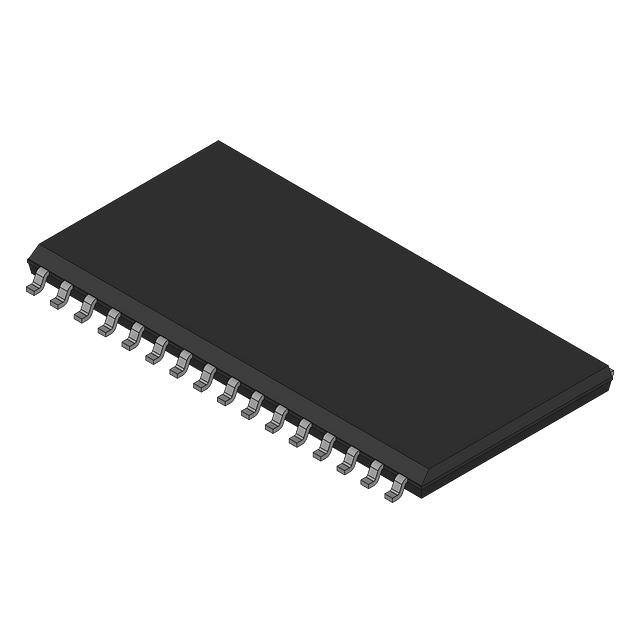
引脚分配:STK14D88有48引脚SSOP和32引脚SOIC两种封装形式。包括电源引脚(VCC和VSS)、地址输入(A0-A14)、数据输入输出(DQ0-DQ7)、控制引脚(E、W、c)、硬件存储忙信号(HSB)、自动存储电容器(VCAP)以及无连接引脚(NC)。
参数特性:
- 读访问和读写周期时间分别为25、35、45纳秒。
- 无限的读/写耐久性。
- 自动非易失性存储,以防断电。
- 非易失性存储可在硬件或软件控制下进行。
- 通电时自动恢复到SRAM。
- 长达20年的非易失性数据保留。
- 单一3.0V ±20%,-10%电源供应。
- 商用、工业温度范围。
- 小型SOIC和SSOP封装(符合RoHS)。
功能详解:
- STK14D88是首款单片非易失性存储器,提供无限的写入和读取。
- 包括逻辑块图、存储/调用操作、模式选择和数据保护等详细操作说明。
- 包括最佳实践、低平均活跃功耗、噪声考虑和防止自动存储的指导。
应用信息:由于其独特的非易失性特性,STK14D88适用于需要断电保护数据的应用场合。
封装信息:提供两种不同引脚数的封装选项,以适应不同的应用需求。


 工商网监
湘ICP备2023018690号
工商网监
湘ICP备2023018690号
