The Leader in High Temperature
Semiconductor Solutions
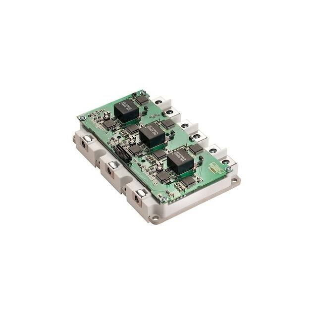
3-Phase 1200V/450A SiC MOSFET
Intelligent Power Module
CXT-PLA3SA12450A-Preliminary Datasheet
Version: 1.9
General description
CXT-PLA3SA12450A is
a 3-phase
1200V/450A SiC MOSFET Intelligent
Power Module integrating the power
switches and the gate driver based on
CISSOID HADES2® chipset.
With its pin fin baseplate, this module
addresses high power density water
cooled converters offering a SiC power
module designed for operation at high
junction temperature (up to 175°C). This
solution gives access to the full benefits of
PUBLIC
Doc. PDS-192038 V1.9
SiC technology to achieve high power
density thanks to low switching losses and
high temperature operation.
The integration of the gate driver together
with the power module give direct access
to a fully validated and optimized solution
in terms of switching speed and losses,
robustness againt dI/dt and dV/dt and protection of the power stages (Desat, UVLO,
AMC, SSD).
WWW.CISSOID.COM
9-Dec-21
1 of 22
�3-Phase 1200V/450A SiC MOSFET Intelligent Power Module
Preliminary Datasheet
Key Features
• VDS breakdown voltage: 1200V
• Single power supply (VCC):
• Low RDSON typ 3.25mΩ
1:
-
• Max Continuous current:
-
• Max 125°C operating ambient
temperature (gate driver)
450A typ. @ Tc=25°C
350A typ. @ Tc=90°C
• Isolation (primary – secondary):
• Thermal resistance (J2C):
-
-
0.13 °C/W typ.
-
-
Eoff: 7.05 mJ
-
• Isolation (baseplate – power pins):
3600VAC @50Hz (1min)
• Common mode transient immunity:
-
>50kV/µs
• Dimensions:
-
5V Schmitt trigger input
Active-High (Active-Low as an
option)
• Open-drain fault reporting:
• Switching frequency: 50kHz Max 2
-
typ 11pF per phase
• PWM input signal
• Switching Energy@ 600V/300A:
Eon: 8.42 mJ
3600VAC @50Hz (1min)
• Parasitic capacitance:
• Max 175°C operating junction
temperature (power devices)
-
+12V to +18V
104(W) x 154(L) X 34(H) (all in mm)
-
per phase
per side as an option
• Turn-On/Off delay: 180ns typ.
• Under voltage lockout (UVLO)
-
On VCC
On internally generated secondary supplies
• Desaturation protection
• Weight: 590g
• Soft Shutdown turn-off (SSD)
• Negative gate drive (-3V)
• Active Miller Clamping (AMC)
• Gate-Source Short-circuit Protection
1
Package resistance excluded
With Gate driver temperature derating from 25KHz
to 50KHz (see curve at page 17)
2
Ordering Information
Product Name
CXT-PLA3SA12450A
PUBLIC
Doc. PDS-192038 V1.9
Ordering Reference
CXT-PLA3SA12450AA
WWW.CISSOID.COM
Marking
CXT-PLA3SA12450AA
9-Dec-21
2 of 22
�3-Phase 1200V/450A SiC MOSFET Intelligent Power Module
Preliminary Datasheet
Block diagram
VDCW+
VX-WT
VREF
FLT-WT
VREF
WH-WT
X
PWM-WT
CLK
DC/DC
VDC-
VCC
WL-WT
VH-WT
VX-WT
W
VL-WT
VH-WB
GND
VDC-
VX-WB
VL-WB
VX-WB
VREF
FLT-WB
VREF
VH-WB
X
PWM-WB
CLK
VL-WB
VDCV+
VX-VT
VREF
FLT-VT
VDCW-
VREF
VH-VT
X
PWM-VT
CLK
DC/DC
VDC-
VCC
VL-VT
VH-VT
VX-VT
V
VL-VT
VH-VB
GND
VDC-
VX-VB
VL-VB
VX-VB
VREF
FLT-VB
VREF
VH-VB
X
PWM-VB
CLK
VL-VB
VDCU+
VX-UT
VREF
FLT-UT
VDCV-
VREF
VH-UT
X
PWM-UT
CLK
DC/DC
VL-UT
VH-UT
VDC-
VCC
VX-UT
U
VL-UT
VH-UB
GND
VDCVL-UB
FLT-UB
VX-UB
VX-UB
VREF
VREF
VH-UB
X
PWM-UB
CLK
VL-UB
PUBLIC
Doc. PDS-192038 V1.9
WWW.CISSOID.COM
VDCU-
9-Dec-21
3 of 22
�3-Phase 1200V/450A SiC MOSFET Intelligent Power Module
Preliminary Datasheet
Pinout3
“VDCU+, VDCV+, VDCW+”, “VDCU-, VDCV-, VDCW-” are not connected to each other internally
3
PUBLIC
Doc. PDS-192038 V1.9
WWW.CISSOID.COM
9-Dec-21
4 of 22
�3-Phase 1200V/450A SiC MOSFET Intelligent Power Module
Preliminary Datasheet
Pinout (cnt’d)
Interface
Pin
Pin name
VDCU+
VDCUVDCV+
VDCVVDCW+
VDCWU
V
W
Description
U Phase positive power supply
U Phase negative power supply
V Phase positive power supply
V Phase negative power supply
W Phase positive power supply
W Phase negative power supply
Half-Bridge output U
Half-Bridge output V
Half-Bridge output W
Pin 1
Pin 2
PWM-UT
PWM-UB
Pin 3
TEMP-U
Pin 4
RSTN
Pin 5
Pin 6
Pin 7
Pin 8
PWM-VT
VDCM
PWM-VB
GND
Pin 9
FLT-T-V
Pin 10
GND
Pin 11
FLT-B-U
Pin 12
VCC
Pin 13
TEMP-V
Pin 14
Pin 15
Pin 16
Pin 17
VCC
PWM input high-side phase U
PWM input low-side phase U
Phase U temperature measurement
output
Reset signal (active low); while low,
forces all PWM to inactive state
PWM input high-side phase V
DC BUS voltage monitoring output
PWM input low-side phase V
Gate driver negative power supply
Phase V fault output or 3 phase
high-side fault output
Gate driver negative power supply
Phase U fault output or 3 phase
low-side fault output
Gate driver positive power supply
Phase V temperature measurement
output
Gate driver positive power supply
GND
FLT-W
Pin 18
TEMP-W
Pin 19
Pin 20
PWM-WT
PWM-WB
POWER
CONTROL
PUBLIC
Doc. PDS-192038 V1.9
Gate driver negative power supply
Phase W fault output
Phase W temperature measurement output
PWM input high-side phase W
PWM input low-side phase W
WWW.CISSOID.COM
9-Dec-21
5 of 22
�3-Phase 1200V/450A SiC MOSFET Intelligent Power Module
Preliminary Datasheet
Max Absolute Ratings
“SiC Power MOSFET’s”
Parameter
Symbol
Drain – Source Voltage
VDS
MOSFET Continuous Drain Current
Pulsed Drain Current
Junction temperature
Case and Storage temperatures
Stray Inductance
ID
IDpulse
Tj
TC,TSTG
LStray
Package resistance @ 25°C4
Clearance distance
Creepage distance
CTI-Comparative Tracking Index
Mounting Torque
Weight
4
MP
MBP
g
Condition
Tj=25°C
Tj=175°C
VGS =15V, TC=25°C, Tj15
mm
min 175
4
2
590
N-m
N-m
g
Package resistance temperature coefficient: 0.39%/°C
PUBLIC
Doc. PDS-192038 V1.9
WWW.CISSOID.COM
9-Dec-21
6 of 22
�3-Phase 1200V/450A SiC MOSFET Intelligent Power Module
Preliminary Datasheet
Max Absolute Ratings
“Gate Driver”
Parameter
VCC-GND
PWM-XT/PWM-XB/RSTN wrt GND
FLT-B-U/ FLT-T-V/FLT-W wrt GND
Min.
-0.5
-0.5V
-0.5V
175
CTI-Comparative Tracking Index
Junction Temperature
Storage and Operating Temperature
ESD Rating (Human Body Model)
between VCC/GND/PWM-XT/PWM-XB/RSTN/FLT-X pins5
-40
1.5
Max.
18
5.5
18
Units
V
V
V
175
125
°C
°C
kV
Max.
Units
Isolation
Parameter
VDCX+/VDCX-/U/V/W wrt
to VCC/GND/PWMXT/PWM-XB/FLT-X
Any of “VDCX+/VDCX/U/V/W/VCC/GND/PWMXT/PWM-XB/FLT-X wrt to
baseplate
Parasitic capacitance
Condition
Min.
AC @50Hz (for 1mn)
Typ.
3600
V
@ 1000VDC
>1
GΩ
Between high-side and primary (per phase)
11
pF
DC Bus Voltage Monitoring
Parameter
Symbol
DC BUS voltage monitoring output
Condition
VDCM
Typ
Unit
0.0033*Diff(VDCV+,VDCU-)
V
Temperature Monitoring
Parameter
Temperature monitoring output
NTC resistance
Symbol
TEMP-U
TEMP-V
TEMP-W
NTCR
Condition
Typ
Unit
NTCR (Ohm)*5/( NTCR (Ohm)+1500)
V
5000
Ω
TNTC=25°C
Steinhart-Hart Coefficients for NTCR versus Temperature computation:
1/(TNTC-273.15) = A+B*ln(R)+C*ln3(R)
TNTC< (273.15+25)K
TNTC> (273.15+25)K
A
9.931*10-4
9.923*10-4
B
2.658*10-4
2.664*10-4
C
1.563*10-7
1.496*10-7
5
Because of functional isolation requirement between «VDCX+/VDCX-/U/V/W» and « VCC/GND/PWM-XT/PWMXB/FLT-X » pins, no ESD performance can be guaranteed between those 2 pin groups.
PUBLIC
Doc. PDS-192038 V1.9
WWW.CISSOID.COM
9-Dec-21
7 of 22
�3-Phase 1200V/450A SiC MOSFET Intelligent Power Module
Preliminary Datasheet
Electrical Characteristics ”Power module”
Unless otherwise stated: (VCC-GND)=15V, TC=25°C. Bold underlined values indicate values over the
whole temperature range (-40°C < TJ < +175°C).
“SiC Power MOSFET’s”
Parameter
Symbol Condition
Tj=25°C ; IDS = 0.02A; VDS = VGS
Threshold voltage
VTH
Tj=175°C ; IDS = 0.02A; VDS =
VGS
VGS =-3V, VDS=1200V, Tj=25°C
Drain cut-off current
IDSS
VGS =-3V, VDS =1200V, Tj=175°C
VGS =15V, ID=300A, Tj=25°C
Static
drain-to-source
reRDSon
sistance6
VGS =15V, ID=300A, Tj=175°C
Breakdown
drain-to-source
VBRDS VGS =-3V; IDS = 500 µA
voltage (DC characterization)
Input capacitance
CISS
VGS =0VDC, VDS =600VDC
f = 100 kHz
Output capacitance
COSS
VAC = 25mV
Feedback capacitance
CRSS
Turn-on delay time
Td(ON)
Rise time
Tr
Turn-off delay time
Td(OFF) VDS=600V; VGS= -3/15V;
IDS = 300A; L = 50µH
Fall time
Tf
Turn-On Switching Energy
Eon
Turn-Off Switching Energy
Eoff
Gate to Source Charge
QGS
Tj=25°C ;VDS= 600V;
Gate to Drain Charge
QGD
IDS = 300A; VGS = -3/15V
Total Gate Charge
QG
TJ=25°C
Short-circuit protection threshISCth
TJ=175°C
old
Maximum short-circuit duration
tSC
Min
1.8
Typ
2.15
Max
3.5
Unit
V
1.7
V
1
50
3.25
5.15
µA
µA
mΩ
mΩ
4
1200
V
30
1.3
76
74
104
213
40
8.42
7.05
292
285
910
1145
750
nF
nF
pF
ns
ns
ns
ns
mJ
mJ
nC
nC
nC
2
µs
A
A
“SiC Reverse Diode”
Parameter
Diode Forward Voltage
Symbol Condition
Tj=25°C ; ISD = 300A; VGS =-3V
VF
Tj=175°C ; ISD = 300A; VGS =-3V
Continuous Diode Forward Current
Diode Pulse Current
Typ
5.18
4.5
Max
Unit
V
V
ISD,DC
VGS =-3V, Tf=25°C, Tj LOW
Non Overlap delay LOW => HIGH
PWM data path
PWM frequency8
Duty cycle
Anti-glitch filter window
Propagation delay (PWM-XB/PWM-XT
→U/V/W) (50% to 10%)
Propagation delay (PWM-XB/PWM-XT
→ U/V/W) (50% to 10%)
50
100
500
kHz
%
ns
180
ns
600
ns
0
Direct Mode; excluding anti-glitch filter
delay
Local Mode; excluding anti-glitch filter
delay
Fault latching time
Timer value (Primary or Secondary
faults)
Timer variation
Under-voltage Lockout on VCC (UVLO_P)
UVLO_P High Threshold
UVLO_P Low Threshold
Delay from UVLO_P detection to FLT-X
@ fault level
Under-voltage Lockout on secondaries gate driver supplies(UVLO_S)
UVLO_S High Threshold
UVLO_S Low Threshold
Delay from UVLO_S detection to FLT-X
@ fault level
Desaturation detection (DESAT_H, DESAT_L)
Desaturation Threshold
wrt to power switch source
Desaturation Blanking time
Delay from
Desaturation detection to
FLT-X in fault state
Soft Shutdown gate fall time
VGS from 15V to 0V
8
14
-30
ms
+25
%
9.75
8.2
V
V
200
ns
16.8
15.5
V
V
600
ns
4.6
1
V
µs
600
ns
1
µs
Please refer to section Gate driver temperature derating for operation above 25kHz (page 17)
PUBLIC
Doc. PDS-192038 V1.9
WWW.CISSOID.COM
9-Dec-21
9 of 22
�3-Phase 1200V/450A SiC MOSFET Intelligent Power Module
Preliminary Datasheet
Typical performances (per switch)
Figure 1: Drain current vs VDS
(VGS=15V, tp < 200µs)9
Figure 2: On-state drain source resistance
vs. Drain current (VGS =15V, tp < 200µs)9
Figure 3: Normalized on-state drain source
resistance (IDS=300A, VGS =15V, tp < 200µs)9
Figure 4: Drain current vs VGS voltage
(VDS=20V, tp < 200µs)
Figure 5 : 3rd quadrant characteristics
(VGS=15V, tp < 200µs) 9
Figure 6: 3rd quadrant characteristics (VGS=3V, tp < 200µs) 9
9
Package resistance excluded
PUBLIC
Doc. PDS-192038 V1.9
WWW.CISSOID.COM
9-Dec-21
10 of 22
�3-Phase 1200V/450A SiC MOSFET Intelligent Power Module
Preliminary Datasheet
Typical performances (per switch) (cnt’d)
Figure 7: Typical capacitances vs VDS
(Tj=25°C ; f = 100 kHz, VAC =25mV)
Figure 8 : Typical capacitances vs VDS
(Tj=25°C ; f = 100 kHz, VAC =25mV)
Figure 9:Threshold vs temp (IDS=20mA; VGS=VDS)
Figure 10 : Switching Energy
Figure 11 : Reverse Recovery Energy
Figure 12 : Max dV/dt vs Drain current
VDS
IDS
10% VDS
10% VDS
10% IDS
10% IDS
ESW (on)
Figure 13 : Max Turn-off dI/dt vs Drain current
PUBLIC
Doc. PDS-192038 V1.9
ESW (on)
Figure 14 : Switching energy computation
WWW.CISSOID.COM
9-Dec-21
11 of 22
�3-Phase 1200V/450A SiC MOSFET Intelligent Power Module
Preliminary Datasheet
Typical performances (per switch) (cnt’d)
Figure 15: MOSFET Junction to Case Thermal Impedance
Figure 16: Forward Bias Safe Operating Area (FBSOA)
Figure 17 : Reverse Bias Safe Operating
Area (RBSOA)
Figure 18: Continuous Drain Current Derating vs Case temperature
Figure 19 : Maximum Power Dissipation Derating vs Case temperature
Figure 20 : Typical Output Current Capability
vs Switching Frequency (Inverter Application)
PUBLIC
Doc. PDS-192038 V1.9
WWW.CISSOID.COM
9-Dec-21
12 of 22
�3-Phase 1200V/450A SiC MOSFET Intelligent Power Module
Preliminary Datasheet
Gate Driver Circuit Functionality
Under-Voltage Lockout (UVLO)
Description
Main features of the CXT-PLA3SA12450A
gate driver are:
- Isolated data transmission (robust to
high dV/dt) (data and fault) on both
high and low side channels
- Adjustable fault timer with automatic
restart
- Safe start-up sequence through monitoring of the main supply (UVLO) and
of the voltage regulators output
(through Power-Good function)
- Permanent and programmable Under-Voltage Lockout (UVLO) monitoring on external and internally generated power switch supplies
- Desaturation detection function with
programmable blanking time and
threshold protecting power switches
in case of abnormal current levels
- Soft-Shutdown transistor and control
performing power device graceful
shutdown in case of fault and so preventing too high dI/dt in the power
stage
- Flyback DC-DC converter (one per
phase) with cycle-by-cycle current
limit for short circuit protection
- High-precision (typ 3%) high-level
gate voltage generation
- Single-ended Schmitt-trigger PWM
inputs
- Open-drain low-ohmic (typ. 25Ω) fault
output
- Support of 2 separate incoming PWM
channels and of locally generated
non-overlapped PWM signals (per
phase) (configuration via jumper)
- Configurable 500ns (typ) spike filter
on incoming PWM signal for enhanced noise robustness
- Anti-overlap protection on incoming
PWM signals
- Gate-2-Source short-circuit protection
- Support of 100% duty-cycle PWM
- Very low parasitic capacitance between secondaries and primary
PUBLIC
Doc. PDS-192038 V1.9
CXT-PLA3SA12450A gate driver board
monitors constantly:
-
VCC power supply
High-side secondary supplies (typ
+15V/-3V)
Low-side secondary supplies (typ
+15V/-3V)
At primary side, the monitored power supply is “VCC-GND”; to avoid oscillation
when (VCC-GND) is close to the UVLO
threshold, a hysteresis is implemented.
At each secondary side, the monitored
power
supply
is
“VDD_L-VSS_L”/
“VDD_H-VSS_H”; to avoid oscillation
when (VDD_x-VSS_x) is close to the
UVLO threshold, a hysteresis is implemented.
Refer to the chapter Fault Management for
details about fault behavior and management.
On-board power supplies
The on-board isolated power supply (per
phase) is a regulated flyback DC-DC converter providing both high-side and lowside channels with the positive and negative supply voltages required to drive the
power FETs. It offers high voltage isolation
between the channels, high dV/dt sustainability and very low parasitic capacitance.
Cycle-by-cycle current monitoring at primary side is implemented to protect the
board against short-circuit.
High accuracy (typ 3%) is achieved on all
secondary positive supplies.
WWW.CISSOID.COM
9-Dec-21
13 of 22
�3-Phase 1200V/450A SiC MOSFET Intelligent Power Module
Preliminary Datasheet
Interface towards controller
Desaturation detection
PWM inputs
The purpose of the desaturation function is
to detect that the voltage at the drain of
the power switch, in “ON” state, is higher
than a given threshold. This informs the
logic part of the system about possible
damage of the power arm (e.g. a short
circuit at the arm level leading to an overcurrent in the power switch).
PWM-XB and PWM-XT input interface is
based on 5V Schmitt-Trigger input receivers and is Active High. Active Low is
available as an option.
CXT-PLA3SA12450A gate driver board
implements 2 protection functions on the
PWM data paths:
-
Anti-glitch: any negative or positive glitch on PWM-XB/PMW-XT
signals smaller than a programmed value is ignored by the
board; this is increasing immunity
of incoming signals against external noise; the PWM signals are
delayed by the corresponding antiglitch time
tMINPW (ns)= 1* [CGLIx (pF)]
-
The desaturation threshold (voltage on
transistor VDS) is configured by on-board
resistors and can be tuned according to
the table below.
Rdesat value
Anti-overlap: this circuit prevents
PWM-XB and PMWH from being
active at the same time.
FAULT outputs
0KΩ
5KΩ
10KΩ
12KΩ
Desat threshold (V)
25°C
125°C
1.18
1.47
2.6
2.87
4.01
4.27
4.6
4.83
(default)
The output buffers operate as an opendrain driver with a very low Ron resistance
(typ. 25Ω), enabling the use of low value
pull-up resistance for increased noise immunity.
An on-board 10k pull-up resistance (connected to internal 5V supply) is present on
each fault output to ease initial testing.
By default, there is one fault output per
phase (one fault per side [top/bottom] is
available as an option).
15KΩ
20KΩ
5.42
6.84
5.66
7.06
At system level, the de-saturation detection should only be taken into account after a defined time following the low-to-high
transition on the power device gate. This
“blanking” time tDESAT_D is implemented
and adjusted by an on-board capacitor
CDESATD (68pF installed) and can be calculated as follows:
tDESATD (ns)= 14* [CDESATD (pF) + 7]
Isolated data transmission
CXT-PLA3SA12450A gate driver board
uses integrated digital isolators. Those
devices provide isolation, immunity against
high dV/dt and low parasitic capacitance.
In case no power supply is present at the
secondary side, a fault is generated at the
primary side.
PUBLIC
Doc. PDS-192038 V1.9
The sensing of the power device drain
voltage is performed through a high voltage sensing diode whom cathode is connected to the power switch drain and
whom anode is connected to a current
source (typ 2mA) and a sensing circuit.
If after tDESAT_D time, the DESAT comparator output indicates that the transistor VDS
level is higher than the programmed
threshold value, an internal DESAT fault is
generated. Refer to the chapter Fault
Management for details about fault behavior and management.
When the desaturation fault is detected,
the power module gate is gracefully discharged thanks to the Soft-Shutdown circuit to avoid high dI/dt at power module
turn-off
WWW.CISSOID.COM
9-Dec-21
14 of 22
�3-Phase 1200V/450A SiC MOSFET Intelligent Power Module
Preliminary Datasheet
Active Miller Clamping
In case of high positive dV/dt and despite
the negative drive of the power module
gate, a parasitic turn-on of the gate could
take place, inducing shoot-through current
on the power arm.
To prevent this, CXT-PLA3SA12450A gate
driver board implements an Active Miller
Clamping function by bypassing the gate
resistance with a low ohmic path (implemented with a transistor) when the gate is
driven negative.
This transistor also helps to limit the amplitude of negative kick on the power module
gate in case of negative dV/dt.
Fault Management
The primary fault state is combined with
the faults returned by the secondary devices according to Table 1.
Prim
fault
No
No
No
No
Yes
High-side
fault
No
No
Yes
Yes
Yes or No
FLT-X
No fault
Fault
Fault
Fault
Fault
Table 1: FAULT aggregation table
At each of the secondary side, fault is
generated by any of those situations:
-
Fault management is taking place on each
phase independently.
At primary side, fault is generated by any
of those situations:
Low-side
fault
No
Yes
No
Yes
Yes or No
-
Power supply is below the UVLO
threshold
Secondary voltage regulator (5V)
output voltage is below the PowerGood threshold
Desaturation situation is detected
by the DESAT comparator
Main power supply (VCC) is below
the UVLO threshold
Primary linear voltage regulator
(generating the 5V output required
by the on-board logic) is below the
internal Power Good level
Those faults are internally combined to
generate a unique fault signal. This internal fault signal is latched for 14msec.
While the fault is latched, the gate driver is
turned off. At the transition between “no
fault” and “fault” situation, the gate driver
circuit is gracefully shut down.
Those faults are internally combined to
generate a unique fault signal. This internal fault signal is latched for 14msec.
After the predefined latch time period, the
gate driver circuit returns to normal operation:
-
While the fault is latched:
-
-
Both FLT-X pins are tied to “0”
Both power switches are turned off
On board DC-DC is off
-
After the predefined latch time period, the
phase controller will attempt to return to
normal operation:
- If the fault is still present, the phase
will stay in the fault state till the fault
disappears
- If the fault disappeared (e.g. temporary UVLO situation), the phase will
go out of FAULT state and return to
normal operation (DC-DC turned on
and data paths active); still, on the
PWM path, transition to normal operation will happen on the next positive edge of the incoming PWM signal.
PUBLIC
Doc. PDS-192038 V1.9
WWW.CISSOID.COM
If the fault is still present, the gate
driver is kept turned off till the fault
disappears
If the fault disappeared (e.g. temporary UVLO situation), normal
operation will resume on the next
positive edge of incoming PWM
signal
9-Dec-21
15 of 22
�3-Phase 1200V/450A SiC MOSFET Intelligent Power Module
Preliminary Datasheet
RSTN (Reset) behaviour
While in Low-State, pin RSTN forces all
PWM input signals to “0”, turning off all
SiC MOSFET gates in Direct mode and
turning off the High-Side SiC MOSFET
and keeping Low-Side SiC MOSFET on in
Local Mode
Protections
CXT-PLA3SA12450A gate driver is protected on each channel against:
-
Gate overvoltage
Gate undervoltage
Gate-source permanent
circuit
When in Local Mode, an on-board capacitance (Cnovd) defines the non-overlap
delay according to following formula:
tNOV_D (ns)=5.5 * CNOVD (pF)
Board power dissipation
Current consumption of the CXTPLA3SA12450A
gate
driver
board
(VCC=15V; VDCX+=0V) can be computed
as follows:
𝐼𝑖𝑛 = 170𝑚𝐴 + 8.4 ∗ 𝐹𝑠
Where:
short-
-
Non-Overlap Generation
CXT-PLA3SA12450A gate driver board
offers 2 modes of operation:
-
-
Direct Mode: PWM-XB and PWMXT are generated independently
outside CXT-PLA3SA12450A gate
driver board. In this case, proper
non overlapping must be generated externally.
Local Mode: PWM-XB and PWMXT are generated from one input
signal (PWM-XT) and proper non
overlapping timing is managed locally on each phase of CXTPLA3SA12450A gate driver board
(cfr Figure 21)
PWM-XT
G_HS
G_LS
tNOV_D
Iin: Input current (in mA) (wrt to VCC =
15V)
Fs: Switching frequency (in kHz)
The duty cycle of the PWM-XB/PWM-XT
signals has almost no influence on the
current consumption (assuming PWM-XB
and PWM-XT duty cycles are complementary).
To stay within specifications of the internal
secondary voltages, the maximum average Iin current should be 1000 mA (for
VCC =15V).
Temperature measurement
Temperature of each phase is measured
using an NTC resistance mounted on the
power module DBC.
The NTC resistance variation with respect
to temperature is reported in Figure 22:
NTC resistance vs tempand obeys to the
formula provided in section Max Absolute
Ratings.
tNOV_D
Figure 21: Local Mode operation
The choice between those 2 modes of operation is made via the 2 pin header jumper JP1 (located at primary side, one per
phase):
-
JP1 ON: Local mode
JP1 OFF: Direct mode
Figure 22: NTC resistance vs temp
PUBLIC
Doc. PDS-192038 V1.9
WWW.CISSOID.COM
9-Dec-21
16 of 22
�3-Phase 1200V/450A SiC MOSFET Intelligent Power Module
Preliminary Datasheet
The NTC resistance value is converted
into an analog voltage fed to the connector
pins TEMP-U, TEMP-V, TEMP-W. Figure
23: TEMP-X voltage vs tempshows the
relationship between TEMP-X voltage and
NTC temperature.
5
4.5
Cooler circuit pressure drop
Cissoid offers a reference cooler kit (ordering code: ACC-PLA1008) enabling fast
prototying and validation by customers.
The graph below reports the pressure drop
in function of the cooling fluid flow rate
(fluid temperature: 60°C, fluid: 50% ethylene glycol, 50% water
TEMP-X pin voltage (V)
4
3.5
3
2.5
2
1.5
1
0.5
0
-55
-5
45
95
145
195
Temperature (°C)
Figure 23: TEMP-X voltage vs temp
Gate driver temperature derating
Figure 25: Pressure drop in cooling circuit
The CXT-PLA3SA12450A gate driver has
been designed to operate at 125°C ambient upto 25kHz switching frequency.
Above 25 kHz, a derating according to the
graph below needs to be applied.
Figure 24: Gate driver temperature derating
PUBLIC
Doc. PDS-192038 V1.9
WWW.CISSOID.COM
9-Dec-21
17 of 22
�3-Phase 1200V/450A SiC MOSFET Intelligent Power Module
Preliminary Datasheet
Timing Diagrams
Figure 26 illustrates the CXT-PLA3SA12450A gate driver board low-side driver dynamic behavior in normal operation and fault conditions.
Normal
Case
PWM-XB
1
Fault
UVLO
Normal
Case
6
2
7
G_LS
UVLO
3
FLT-X
Internal timer
4
Normal
Case
PWM-XB
1
tFLTD
5
FAULT
Desat
Normal
Case
3
7
8
G_LS
D_LS
tDESATD
DESAT
BLANK tDESATD
FLT-X
2
4
Internal timer
5
tFLTD
6
Figure 26: Timing diagram CXT-PLA3SA12450A low-side gate driver behaviour
In Normal operation
In DESAT fault situation
On PWM-XB rising edge (1), rising edge is
generated on G_LS (after propagation delay through CXT-PLA3SA12450A gate
driver board).
After rising edge on G_LS, low-side power
module is turned ON and midpoint node is
going to “0” state (voltage equals to Ron *
current flowing through the power device).
D_LS node is also pulled down and after
blanking time (tDESAT_D), no desaturation
fault is detected and FAULTL remains
high.
On PWM-XB rising edge (3), rising edge is
generated on G_LS (after propagation delay through CXT-PLA3SA12450A gate
driver board)
After rising edge on G_LS, low-side power
module is turned ON; because of a desaturation fault, D_LS node does not reach its
normal “0” level. Thanks to the DESAT
comparator, CXT-PLA3SA12450A gate
driver board detects this fault situation and
turns off gracefully G_LS. Power device is
turned off. FAULTL signal is pulled down.
Fault is cleared after fault timer expiry.
On PWM-XB falling edge (2), falling edge
is generated on G_LS (after propagation
delay through CXT-PLA3SA12450A gate
driver board)
After falling edge on G_LS, the low-side
power device is turned OFF.
PUBLIC
Doc. PDS-192038 V1.9
WWW.CISSOID.COM
9-Dec-21
18 of 22
�3-Phase 1200V/450A SiC MOSFET Intelligent Power Module
Preliminary Datasheet
In UVLO fault situation
Glossary
UVLO status is monitored inside the secondary devices (and inside primary device
as well; for clarity, only secondary UVLO
situation is described here). When UVLO
comparator (5) detects an under-voltage
situation, G_LS is gracefully shut down
FAULTL signal is pulled down. Fault is
cleared after fault timer expiry.
Name
D_HS
S_HS
G_HS
D_LS
S_LS
G_LS
PUBLIC
Doc. PDS-192038 V1.9
WWW.CISSOID.COM
Description
Drain of any high-side switch
Source of any high-side
switch
Gate of any high-side switch
Drain of any low-side switch
Source of any low -side
switch
Gate of any low -side switch
9-Dec-21
19 of 22
�3-Phase 1200V/450A SiC MOSFET Intelligent Power Module
Preliminary Datasheet
Mechanical drawing
PUBLIC
Doc. PDS-192038 V1.9
WWW.CISSOID.COM
9-Dec-21
20 of 22
�3-Phase 1200V/450A SiC MOSFET Intelligent Power Module
Preliminary Datasheet
Physical dimensions (mm)
Base plate material: AlSiC
Power pins finish: Ni
Gate driver control pins finish: Au
Gate driver control connector: Molex 87831-2020
Item
Baseplate fixing screws
DC Bus Power connector
bolts
Phase power connector
bolts
Gate driver female counter
connector board-2-cable
Gate driver female counter
connector board-2-board
PUBLIC
Doc. PDS-192038 V1.9
Recommended reference
M4x10 ISO 7380-2 A2 TX
M6x12 ISO 7380-2-A2-TX
M6x12 ISO 7380-2-A2-TX
Comments
Assumes min 0.7 mm DC
power connector thickness
Assumes min 1.6 mm phase
connector thickness
Molex 51110 SERIES
Molex 78787-2054(Tin) or
79107-7009(Gold).
WWW.CISSOID.COM
9-Dec-21
21 of 22
�3-Phase 1200V/450A SiC MOSFET Intelligent Power Module
Preliminary Datasheet
Contact & Ordering
CISSOID S.A.
Headquarters and
contact EMEA:
CISSOID S.A. – Rue Francqui, 3 – 1435 Mont Saint Guibert - Belgium
T : +32 10 48 92 10 – F : +32 10 88 98 75
Email : sales@cissoid.com
Sales
Representatives:
Visit our website: http://www.cissoid.com
Disclaimer
Neither CISSOID, nor any of its directors, employees or affiliates make any representations or extend any warranties
of any kind, either express or implied, including but not limited to warranties of merchantability, fitness for a particular
purpose, and the absence of latent or other defects, whether or not discoverable. In no event shall CISSOID, its directors, employees and affiliates be liable for direct, indirect, special, incidental or consequential damages of any kind
arising out of the use of its circuits and their documentation, even if they have been advised of the possibility of such
a damage. The circuits are provided “as is”. CISSOID has no obligation to provide maintenance, support, updates, or
modifications.
PUBLIC
Doc. PDS-192038 V1.9
WWW.CISSOID.COM
9-Dec-21
22 of 22
�