IS31IO7326
DEBOUNCED 8×8 KEY-SCAN CONTROLLER
January 2012
GENERAL DESCRIPTION
FEATURES
The IS31IO7326 is a 64 key, key-scan controller. It
offloads the burden of keyboard scanning from the host
processor. The IS31IO7326 supports keypad matrix of
up to 8×8. Key press and release events are encoded
into a byte format and loaded into a key event register
for retrieval by the host processor.
The IS31IO7326 integrates a debounce function which
rejects false or transient key switch activities. The
_______
interrupt output (INT) is used to signify if there are any
keypad activities.
To minimize power, the IS31IO7326 automatically
enters a low power standby mode when there is no
keypad, I/O, or host activity.
2.4V to 5.5V operation
400kHz I2C serial interface
Available for multi-key press detect
Low 0.3μA (typ.) standby current
Operate in -40°C to +125°C
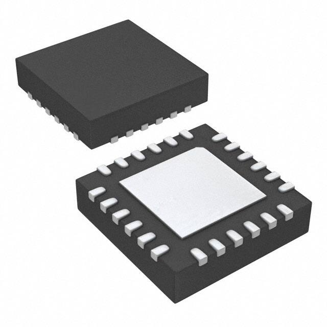
Pb-free 4mm × 4mm QFN-24 package
APPLICATIONS
Keypad of QWERTY type phones
PDAs, games, and other handheld applications
The IS31IO7326 is available in a Pb-free 4mm × 4mm
QFN-24 package.
TYPICAL APPLICATION CIRCUIT
VBattery
100k
VBattery
21
PP0
VCC
PP1
1 F
0.1 F
PP2
PP3
VDD
4.7k
4.7k
PP4
4.7k
PP5
19
20
Micro
Controller
22
23
PP6
SCL
SDA
IS31IO7326
OD0
RST
OD1
OD3
9
AD0
AD1
GND
Figure 1
Lumissil Microsystems – www.lumissil.com
Rev. A, 12/19/2011
3
4
14
15
16
17
5
INT
OD2
24
2
PP7
100k
18
1
OD4
OD5
OD6
OD7
6
7
8
10
11
12
13
Typical Application Circuit
1
�IS31IO7326
PIN CONFIGURATION
Package
Pin Configuration (Top View)
QFN-24
PIN DESCRIPTION
No.
Pin
1~4, 14~17
PP0~PP7
Output ports.
5~8, 10~13
OD0~OD7
Input ports.
9
GND
Ground.
18
AD0
Address setting.
19
SCL
I2C serial clock.
20
SDA
I2C serial data.
21
VCC
Power supply voltage.
22
_______
INT
Interrupt output, active low.
23
________
Reset input, active low.
24
Description
RST
AD1
Address setting.
Thermal Pad
Connect to GND.
Lumissil Microsystems – www.lumissil.com
Rev. A, 12/19/2011
2
�IS31IO7326
ORDERING INFORMATION
Industrial Range: -40°C to +125°C
Order Part No.
Package
QTY/Reel
IS31IO7326-QFLS4-TR
QFN-24, Lead-free
2500
Copyright © 2011 Lumissil Microsystems. All rights reserved. Lumissil Microsystems reserves the right to make changes to this specification and its
products at any time without notice. Lumissil Microsystems assumes no liability arising out of the application or use of any information, products or
services described herein. Customers are advised to obtain the latest version of this device specification before relying on any published information and
before placing orders for products.
Lumissil Microsystems does not recommend the use of any of its products in life support applications where the failure or malfunction of the product can
reasonably be expected to cause failure of the life support system or to significantly affect its safety or effectiveness. Products are not authorized for use in
such applications unless Lumissil Microsystems receives written assurance to its satisfaction, that:
a.) the risk of injury or damage has been minimized;
b.) the user assume all such risks; and
c.) potential liability of Lumissil Microsystems is adequately protected under the circumstances
Lumissil Microsystems – www.lumissil.com
Rev. A, 12/19/2011
3
�IS31IO7326
ABSOLUTE MAXIMUM RATINGS
Supply voltage, VCC
Voltage at any input pin (Except PP0-PP7)
________
-0.3V ~ +6.0V
-0.3V ~ VCC+0.3V
-0.3V ~ +6.0V
-0.3V ~ VCC+0.3V
±100mA
120mA
10mA
10mA
_______
SCL, SDA, AD, RST, INT, OD0-OD3
PP0–PP3
PP source output current
PP/OD sink current
SDA sink current
_______
INT sink current
Continuous power dissipation (TA = 70°C) 24-Pin QFN (Derate
33.2mW/°C over 70°C)
Maximum junction temperature, TJMAX
Storage temperature range, TSTG
Operating temperature range, TA
Solder information, vapor phase (60s)
infrared (15s)
ESD HBM
2.65W
+150°C
-65°C ~ +150°C
-40°C ~ +125°C
215°C
220°C
±4kV
Note: Stresses beyond those listed under “Absolute Maximum Ratings” may cause permanent damage to the device. These are stress ratings
only and functional operation of the device at these or any other condition beyond those indicated in the operational sections of the specifications
is not implied. Exposure to absolute maximum rating conditions for extended periods may affect device reliability.
ELECTRICAL CHARACTERISTICS
TA= -40°C ~ +125°C, VCC = 2.4V ~ 5.5V, unless otherwise noted. Typical values are at TA = 25°C, VCC = 3.3V.
(Note 1)
Symbol
Parameter
Condition
Min.
VCC
Supply voltage
VPOR
Power-on-reset voltage
VCC falling
Standby current
(Interface idle)
Supply current
(Interface running)
SCL,SDA and other digital inputs
at VCC
fSCL = 400kHz
other digital inputs at VCC
ISTB
I+
Typ.
Max.
Units
5.5
V
2.35
V
0.3
1.9
μA
6.5
25
μA
2.4
VIH
Logic “1” input voltage
VIL
Logic “0” input voltage
1.4
V
0.4
V
+0.2
μA
________
IIH, IIL
SDA, SCL, AD0, AD1, RST ,
OD0~OD7 at VCC or GND
Input leakage current
-0.2
Input capacitance
CIN
VOL
________
SDA, SCL, AD0, AD1, RST,
OD0~OD7, PP0~PP7
Logic “0” output voltage
PP0~PP7
_______
(Note 2)
10
VCC = 2.5V, ISINK = 10mA
200
VCC = 3.3V, ISINK = 15mA
240
VCC = 5.0V, ISINK = 20mA
250
180
VOLINT
Output low-voltage INT
ISINK = 5mA
tSCAN
Time to scan key matrix
completely
Configuration Register bit SD = 0
16
Configuration Register bit SD = 1
9
_______
pF
Lumissil Microsystems – www.lumissil.com
Rev. A, 12/19/2011
mV
mV
ms
4
�IS31IO7326
TIMING CHARACTERISTICS
TA = -40°C ~ +125°C, VCC = 2.4V ~ 5.5V, unless otherwise noted. Typical values are at TA = 25°C, VCC = 3.3V.
(Note 3)
Symbol
Parameter
Condition
Min.
Typ.
Max.
Units
400
kHz
fSCL
Serial-clock frequency
tBUF
Bus free time between a STOP and a
START condition
1.3
μs
tHD, STA
Hold time (repeated) START condition
0.6
μs
tSU, STA
Repeated START condition setup time
0.6
μs
tSU, STO
STOP condition setup time
0.6
μs
tHD, DAT
Data hold time
tSU, DAT
Data setup time
100
ns
tLOW
SCL clock low period
1.3
μs
tHIGH
SCL clock high period
Rise time of both SDA and SCL signals,
receiving
Fall time of both SDA and SCL signals,
receiving
0.7
μs
tR
tF
tF, TX
tSP
0.9
(Note 3)
μs
(Note 4)
20 + 0.1Cb
300
ns
(Note 4)
20 + 0.1Cb
300
ns
Fall time of SDA transmitting
(Note 4)
20 + 0.1Cb
250
ns
Pulse width of spike suppressed
(Note 5)
50
Cb
Capacitive load for each bus line
tW
________
ns
400
RST pulse width
pF
500
ns
1
μs
________
________
tRST
RST rising to START condition setup
time
PORT AND INTERRUPT TIMING CHARACTERISTICS
T = -40°C ~ +125°C, VCC = 2.4V ~ 5.5V, unless otherwise noted. Typical values are at TA = 25°C, VCC = 3.3V
(Note 3)
Symbol
Parameter
Condition
Min.
Typ.
Max.
Untis
4
μs
tPV
Port output data valid
CL≤ 100pF
tPSU
Port input setup time
CL≤ 100pF
0
μs
tPH
Port input hold time
CL≤ 100pF
4
μs
tIV
_______
INT input data valid time
CL≤ 100pF
4
μs
tIR
_______
CL≤ 100pF
4
μs
INT reset delay time from acknowledge
Note 1: All parameters are tested at TA = 25°C. Specifications over temperature are guaranteed by design.
Note 2: Guaranteed by design.
Note 3: A master device must provide a hold time of at least 300ns for the SDA signal (referred to VIL of the SCL signal) in order to bridge the
undefined region of SCL’s falling edge.
Note 4: Cb = total capacitance of one bus line in pF. ISINK ≤ 6mA. tR and tF measured between 0.3 × VCC and 0.7× VCC.
Note 5: Input filters on the SDA and SCL inputs suppress noise spikes less than 50ns.
Lumissil Microsystems – www.lumissil.com
Rev. A, 12/19/2011
5
�IS31IO7326
DETAILED DESCRIPTION
I2C INTERFACE
The IS31IO7326 uses a serial bus, which conforms to
the I2C protocol, to control the chip’s functions with two
wires: SCL and SDA. The IS31IO7326 has a 7-bit slave
____
address (A7:A1), followed by the R/W bit, A0. Set A0 to
“0” for a write command and set A0 to “1” for a read
command. The bit A2:A1 are selected by the
connection of AD1/AD0 pin.
The complete slave address is:
Table 1 Slave Address:
Bit
A7:A3
A2
A1
A0
Default
10110
AD1
AD0
0/1
The SCL line is uni-directional. The SDA line is
bi-directional (open-collector) with a pull-up resistor
(typically 4.7kΩ). The maximum clock frequency
specified by the I2C standard is 400kHz. In this
discussion, the master is the microcontroller and the
slave is the IS31IO7326.
The timing diagram for the I2C is shown in Figure 3.
The SDA is latched in on the stable high level of the
SCL. When there is no interface activity, the SDA line
should be held high.
The “START” signal is generated by lowering the SDA
signal while the SCL signal is high (Figure 4). The start
signal will alert all devices attached to the I2C bus to
check the incoming address against their own chip
address.
The 8-bit chip address is sent next, most significant bit
first. Each address bit must be stable while the SCL
level is high.
Lumissil Microsystems – www.lumissil.com
Rev. A, 12/19/2011
Following acknowledge of IS31IO7326, the register
address byte is sent, most significant bit first.
IS31IO7326 must generate another acknowledge
indicating that the register address has been received.
An 8-bit data byte is sent next, most significant bit first.
Each data bit should be valid while the SCL level is
stable high. After the data byte is sent, the IS31IO7326
must generate another acknowledge to indicate that
the data was received.
AD1/AD0 connects to VCC, AD1/AD0=1;
AD1/AD0 connects to GND, AD1/AD0=0;
Figure 2
After the last bit of the chip address is sent, the master
checks for the IS31IO7326’s acknowledge. The master
releases the SDA line high (through a pull-up resistor).
Then the master sends an SCL pulse. If the
IS31IO7326 has received the address correctly, then it
holds the SDA line low during the SCL pulse. If the SDA
line is not low, then the master should send a “STOP”
signal (discussed later) and abort the transfer.
The “STOP” signal ends the transfer. To signal “STOP”,
the SDA signal goes high while the SCL signal is high
(Figure 4).
WRITING TO THE REGISTERS
Transmit data to the IS31IO7326 by sending the device
slave address and setting the LSB to “0”. The
command byte is sent after the address and
determines which registers receive the data following
the command byte (Figure 2).
READING PORT REGISTERS
To read the device data, the bus master must first send
____
the IS31IO7326 address with the R/W bit set to “0”,
followed by the command byte, which determines
which register is accessed. After a restart, the bus
master must then send the IS31IO7326 address with
____
the R/W bit set to “1”. Data from the register defined by
the command byte is then sent from the IS31IO7326 to
the master (Figure 6).
Writing to IS31IO7326
6
�IS31IO7326
SDA
tSU ,D A T
SCL
S
t LO W
tSU ,STA
t H D,DA T
tH D,STA
tH IGH
tSU,STO
t BU F
P
R
tH D,STA
tR
tF
Stop
Condition
Restart Condition
Start Condition
Interface Timing
Figure 3
START and STOP Conditions
Figure 4
Figure 5
Figure 6
Start
Condition
Acknowledge Signal
Reading I/O Ports of IS31IO7326
KEY PRESS/RELEASE
KEY PRESS/RELEASE
INT
16ms
(6ms/8ms)
9ms
(3ms/4ms)
_______
Figure 7
Lumissil Microsystems – www.lumissil.com
Rev. A, 12/19/2011
I N T Timing
7
�IS31IO7326
REGISTER DEFINITION
Table 2 Register Function
Address
Name
Function
Default
Table
08h
Configuration Register
0001 0000
3
10h
Key Status Register
Configure the keypad scan function
Contains the information of the key
events
0000 0000
4
Table 4 10h Key Status Register
Table 3 08h Configuration Register
Bit
D7
D6:D5
D4
D3
D2
D1:D0
Bit
D7
D6
D5:D0
Name
Reserved
ACI
DE
SD
LE
LT
Name
DN
KS
KM
Default
0
00
1
0
0
00
Default
0
0
000000
The Configuration Register is used to configure the
keypad scan function.
The Key Status Register contains the information of the
key events that have been debounced (see the Table 5
of the key mapping).
_______
ACI
Auto Clear INT
00
Auto clear INT disabled
01
Auto clear INT in 5ms
10
Auto clear INT in 10ms
DE
0
1
Input Port Filter Enable
Input port filter disable
Input port filter enable
SD
0
1
Key Scan Debounce Time
Double debounce time (6ms, 8ms)
Normal debounce time (3ms, 4ms)
LE
0
1
Long-pressed Key Detect Enable
Disable
Enable
LT
00
01
10
11
Long-pressed Key Detect Delay Time
20ms
40ms
1s
2s
_______
_______
DN
0
1
Indicate Data Number
One key event to report
More than one key to report
KS
0
1
Key State
Key released
Key pressed
KM
Key Mapping
_______
Lumissil Microsystems – www.lumissil.com
Rev. A, 12/19/2011
KM denotes which of the 64 keys have been
debounced and the keys are numbered as shown in
the Table 5.
When the Key Status Register is read over (DN=0), the
_______
register is set to “0000 0000”, and the INT is cleared.
8
�IS31IO7326
Table 5 Key Mapping (D5:D0)
PP0
PP1
PP2
PP3
PP4
PP5
PP6
PP7
OD0
000000
000001
000010
000011
000100
000101
000110
000111
OD1
001000
001001
001010
001011
001100
001101
001110
001111
OD2
010000
010001
010010
010011
010100
010101
010110
010111
OD3
011000
011001
011010
011011
011100
011101
011110
011111
OD4
100000
100001
100010
100011
100100
100101
100110
100111
OD5
101000
101001
101010
101011
101100
101101
101110
101111
OD6
110000
110001
110010
110011
110100
110101
110110
110111
OD7
111000
111001
111010
111011
111100
111101
111110
111111
Examples
_______
1. If the key PP1-OD3 pressed only, and other keys keep released state, the INT asserts, the data in Key Status
Register would be “0101 1001”;
_______
2. If the key PP4-OD6 released only, and other keys keep released state, the INT asserts, the data in Key Status
Register would be “0011 0100”;
_______
3. If the key PP2-OD4 and PP3-OD7 are pressing, then PP2-OD4 released, the INT asserts, the first data in Key
Status Register would be “1010 0010”, the second data would be “0111 1011”. Then judge the MSB (bit DN) in
_______
the second data is “0”. Data has read over, and INT goes to high.
_______
We must read over the data in Key Status Register when the I N T asserts. When judge the MSB (bit DN) in the data is “0”, stop reading the
Key Status Register. If there are some keys connected to the same OD port pressing at the same time, IS31IO7326 only can detect the first
pressed key and others will ignore.
Lumissil Microsystems – www.lumissil.com
Rev. A, 12/19/2011
9
�IS31IO7326
APPLICATION INFORMATION
INPUT AND OUTPUT PORT STRUCTURE
A 100kΩ pull-up resistor will force input port high at
VBattery.
If a change of the state of the keypad is detected, the
keypad would be scanned thrice between the
debounce delay. When the state changes have been
reliably captured, the key event(s) are encoded and
V+
written to temporary key status registers. The INT
asserts when the key event(s) is (are) stored. Reading
the Key Status Register reports the key events in the
order of lowest encoding value to the highest (see
Output
_______
PP0~PP7
Dirver
_______
Table 5). The INT will remain low until all of the key
events are read, with one exception: When the
_______
Auto-Clear INT is enabled, if all of the key event data
_______
GND
Figure 8
Output Port Structure
is not read before the programmed time, the INT will
return high after the programmed time. However the
temporary key status registers will remain unchanged
and the key event data may continue to be read until
another key event is detected.
DEBOUNCE
When the bit SD of the Configuration Register (08h) is
set to “0” and there is a change of the state of the
keypad, the keypad scans first and stores the data in
temporary registers, then waits for about 6ms (3ms)
and scans again, then waits for another 8ms (4ms) and
scans a final time. If the results are the same, the data
is latched into the temporary key status registers and
_______
Figure 9
Input Port Structure
the INT asserted. Otherwise, the scan is halted and
the device returns to standby mode. No data is latched
_______
POWER-ON RESET
The IS31IO7326 contains an integral power-on-reset
circuit that ensures all registers are reset to a known
state on power-up. When VCC rises above 2.4V, the
circuit releases the registers and the I2C interface for
normal operation. When VCC drops to less than VPOR,
the IS31IO7326 resets all register contents to the
default value.
________
RST I2C RESET CONTROL
________
The active-low RST input voids any I2C transaction
involving the IS31IO7326, forcing the IS31IO7326 into
the I2C STOP condition. A reset does not affect the
interrupt output.
into the temporary key status registers and the INTis
not asserted.
LONG-PRESSED KEY DETECT
When the bit LE of the Configuration Register (08h) is
set to “0”, this function is disabled. When LE is set to
“1”, this function is enabled. When a key is pressed for
a long period of time, the chip automatically scans
_______
again after the INT is deasserted. When the key is still
_______
pressed, the INT asserts again and the key event is
latched into the temporary key status registers. The
scanning continues until all of the keys are released.
_______
The delay time between the INT deasserting to the
next scan beginning is set by the Configuration
Register (08h) bits LT.
_______
STANDBY MODE
KEY EVENT INTERRUPT (INT)
When the serial interface is idle, the IS31IO7326
automatically enters standby mode, drawing minimal
supply current.
Once there is key event code latched in the temporary
key status registers, the device produces an interrupt
KEYPAD AUTO SCAN
_______
_______
signal to the MCU on the INT pin. When the INT is
asserted, any keypad state changes are ignored. The
_______
The IS31IO7326 can support an 8×8 matrix keypad
scan. The 8 input ports (OD ports) need a 100kΩ
pull-up resistor for each column, the 8 output ports (PP
ports) for the rows pull low in standby mode.
Lumissil Microsystems – www.lumissil.com
Rev. A, 12/19/2011
INT will remain low until all of the key events are read,
_______
with one exception: When the Auto-Clear INT is
enabled, if all of the key event data is not read before
_______
the programmed time, the INT will return high after
10
�IS31IO7326
the programmed time. However the temporary key
status registers will remain unchanged and the key
event data may continue to be read until another key
event is detected. After all of the key events have been
read, the device returns to standby mode waiting for
the next scan.
_______
AUTO-CLEAR INT FUNCTION
When the ACI bits of the Configuration Register (08h)
are set to “01” or “10”, this function is enabled. Setting
the ACI bits to “00” disables the function. When
THE INPUT PORT FILTER
The bit DE of the Configuration Register (08h) is used
to enable the input port filter. When DE is set to “0”, the
input port filter is disabled, and the chip responds to
any changes at the input port. When DE is set to “1”,
the input port filter is enabled and any glitch shorter
than 100ns is filtered. If the input pulse width is greater
than 100ns, the chip responds (Figure 10).
_______
enabled, the INT would be cleared in 5ms or 10ms
after it asserts if there is no read of the Key Status
Register. The data in
the temporary key status
_______
registers does not change when the INT goes low. The
Key Status Register can be read regardless of whether
_______
_______
the INT is high or not. However, when the INT is
cleared and there is new key event activity before the
old key event data is read, the temporary key status
_______
registers are rewritten and the INT asserts again. In
this case, the previous key event data is lost and only
the new key event(s) can be read.
Lumissil Microsystems – www.lumissil.com
Rev. A, 12/19/2011
Figure 10
Input port debounce function
11
�IS31IO7326
CLASSIFICATION REFLOW PROFILES
Profile Feature
Pb-Free Assembly
Preheat & Soak
Temperature min (Tsmin)
Temperature max (Tsmax)
Time (Tsmin to Tsmax) (ts)
150°C
200°C
60-120 seconds
Average ramp-up rate (Tsmax to Tp)
3°C/second max.
Liquidous temperature (TL)
Time at liquidous (tL)
217°C
60-150 seconds
Peak package body temperature (Tp)*
Max 260°C
Time (tp)** within 5°C of the specified
classification temperature (Tc)
Max 30 seconds
Average ramp-down rate (Tp to Tsmax)
6°C/second max.
Time 25°C to peak temperature
8 minutes max.
Figure 11
Classification profile
Lumissil Microsystems – www.lumissil.com
Rev. A, 12/19/2011
12
�IS31IO7326
TAPE AND REEL INFORMATION
Lumissil Microsystems – www.lumissil.com
Rev. A, 12/19/2011
13
�IS31IO7326
PACKAGE INFORMATION
QFN-24
Note: All dimensions in millimeters unless otherwise stated.
Lumissil Microsystems – www.lumissil.com
Rev. A, 12/19/2011
14
�


 工商网监
湘ICP备2023018690号
工商网监
湘ICP备2023018690号
