NJM12901
SINGLE SUPPLY QUAD COMPARATOR
■ GENERAL DESCRIPTION
The NJM12901 is single-supply quad voltage comparator,
which can operate from 2V supply. The features are low input
offset voltage, low input bias current and low current
consumption. The NJM12901 compare the input signal to 0V
( ground ) due to the Darlington PNP input stage.
The package lineup is DMP and others compact, so that the
NJM12901 is suitable for any kind of signal comparator.
■ FEATURES
● Operating Voltage
● Open Collector Output
● Bipolar Technology
● Package Outline
■ PACKAGE OUTLINE
NJM12901M
NJM12901V
( +2V ~ +14V )
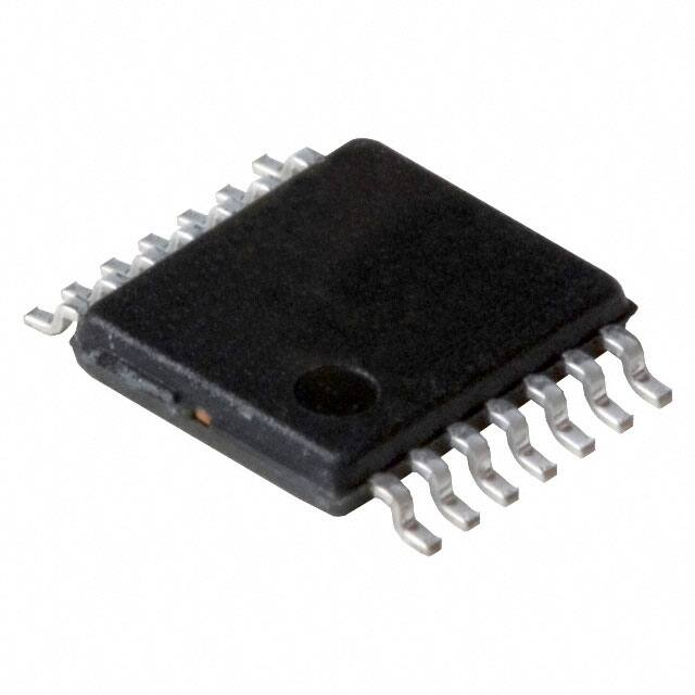
DMP14, SSOP14
■ PIN CONFIGURATION
1
14
2
13
3
A
D
− +
− +
4
11
5
6
12
10
B
C
− +
− +
7
9
8
PIN FUNCTION
1. B OUTPUT
2. A OUTPUT
3. V+
4. A - INPUT
5. A +INPUT
6. B - INPUT
7. B +INPUT
8. C - INPUT
9. C +INPUT
10. D - INPUT
11. D +INPUT
12. GND
13. D OUTPUT
14. C OUTPUT
NJM12901M, NJM12901V
■ EQUIVALENT CIRCUIT ( 1/4 Shown )
V
+ INPUT
+
OUTPUT
− INPUT
GND
Ver.2011-09-20
-1-
�NJM12901
■ ABSOLUTE MAXIMUM RATINGS( Ta=25˚C )
PARAMETER
SYMBOL
+
RATING
UNIT
Supply Voltage
V
15
V
Differential Input Voltage
VID
14 (Note1)
V
Common Mode Input Voltage
VIC
-0.3~+14 (Note1)
V
Power Dissipation
PD
Operating Temperature Range
Storage Temperature Range
Topr
Tstg
DMP14 300
SSOP14 300
-40~+85
-50~+125
mW
°C
°C
(Note1) For supply voltage less than 14V, the maximum input voltage is equal to the supply voltage.
■ ELECTRICAL CHARACTERISTICS( V+=5V,Ta=25˚C unless otherwise specified )
PARAMETER
SYMBOL
Operating Voltage
VOPR
Input Offset Voltage
VIO
Input Offset Current
IIO
TEST CONDITION
Rs=0Ω,Vo≈1.4V
MIN.
TYP.
MAX.
UNIT
2
-
14
V
-
1
4
mV
-
5
50
nA
Input Bias Current
IB
-
30
200
nA
Common Mode Input Voltage Range
VICM
0~3.5
-
-
V
Large Signal Voltage Gain
AV
RL=15kΩ
-
106
-
dB
Response Time
tR
RL=5.1kΩ
-
0.5
-
µs
-2-
Output Sink Current
ISINK
VIN+=0V,VIN-=1V,Vo=1.5V
6
10
-
mA
Output Saturation Voltage
VSAT
VIN+=0V,VIN-=1V,ISINK=3mA
-
80
300
mV
Output Leakage Current
ILEAK
VIN+=0V,VIN-=1V,Vo=5V
-
0.1
1
µA
Supply Current
ICC
RL=∞
-
0.8
1.8
mA
Ver.2011-09-20
�NJM12901
■ TYPICAL CHARACTERISTICS
Supply Current vs. Temperature (Supply Voltage)
Supply Current vs. Supply Voltage
Ta=25ºC
0.8
1.6
1.4
Supply Current Icc [mA]
Supply Current Icc [mA]
0.7
0.6
0.5
0.4
0.3
0.2
0.1
1
0.8
V+=+2V
0.6
0.4
0
0
2
4
6
8
10 12
+
Supply Voltage V [V]
14
16
-50
Input Offset Voltage vs. Supply Voltage
-25
0
25
50
75
100
Ambient Temperature Ta [ºC]
125
Input Offset Voltage vs. Temperature (Supply Voltage)
Ta=25ºC
2.5
2.5
2
Input Offset Voltage VIO [mV]
Input Offset Voltage VIO [mV]
V+=+5V
0.2
0
1.5
1
0.5
0
-0.5
-1
-1.5
2
1.5
V+=+2V, +5V, +14V
1
0.5
0
-0.5
-1
-1.5
-2
-2
0
2
4
6
8
10 12
+
Supply Voltage V [V]
14
16
-50
Common Mode Input Voltage Range
-25
0
25
50
75
100
Ambient Temperature Ta [ºC]
125
Input Bias Current vs. Temperature (Supply Voltage)
V+=+5V
5
120
4
Input Bias Current IB [nA]
Input Offset Voltage VIO [mV]
V+=+14V
1.2
3
2
1
0
-1
-2
-3
100
80
V+=+14V
60
V+=+5V
40
V+=+2V
20
0
2.6
Ver.2011-09-20
2.8
3
3.2
3.4
3.6
Input Voltage Vin [V]
3.8
4
-50
-25
0
25
50
75
100
Ambient Temperature Ta [ºC]
125
-3-
�NJM12901
■ TYPICAL CHARACTERISTICS
Output Saturation Voltage vs. Output Sink Current
(Temperature)
V+=+5V
Input Bias Current vs. Supply Voltage
Ta=25ºC
10
Output Saturation Voltage Vsat [V]
80
Input Bias Current Ib [nA]
70
60
50
40
30
20
10
0
0
2
4
6
8
10 12
+
Supply Voltage V [V]
14
16
Ta=25ºC
0.1
0.001
0.01
100
Output Saturation Voltage Vsat [mV]
200
180
Output Saturation Voltage
Vsat [mV]
0.1
1
10
Output Sink Current Isink [mA]
Output Saturation Voltage vs. Supply Voltage
(Supply Voltage)
(Isink=3mA)
160
140
120
Ta=85ºC
0.01
Output Saturation Voltage vs. Temperature
200
Ta=-40ºC
1
+
V =+2V, +5V, +14V
100
80
60
40
20
0
180
160
140
Isink=6mA
120
100
80
60
40
Isink=3mA
20
0
-50
-25
0
25
50
75
100
Ambient TemperatureTa [ºC]
125
0
2
Pulse Response
4
6
8
10 12
+
Supply Voltage V [V]
14
16
Pulse Response
Vout
1V/div
0.5µs/div
Over Drive 50mV
Vout
Vout
1V/div
0.5µs/div
Over Drive 50mV
Vin
100mV/div
0.5µs/div
Voltage V [V]
VoltageV [V]
Over Drive 5mV
Vout
Over Drive 5mV
Vin
Vin
100mV/div
0.5µs/div
Vin
Time t [µs]
Time t [µs]
[CAUTION]
The specifications on this data book are only given for information,
without any guarantee as regards either mistakes or omissions. The
application circuits in this data book are described only to show
representative usages of the product and not intended for the
guarantee or permission of any right including the industrial rights.
-4-
Ver.2011-09-20
�
很抱歉,暂时无法提供与“NJM12901V-TE1”相匹配的价格&库存,您可以联系我们找货
免费人工找货