0
登录后你可以
  • 下载海量资料
  • 学习在线课程
  • 观看技术视频
  • 写文章/发帖/加入社区
会员中心
创作中心
发布
  • 发文章

  • 发资料

  • 发帖

  • 提问

  • 发视频

创作活动
NJM339CV-TE1

NJM339CV-TE1

  • 厂商:

    NJR(新日本无线)

  • 封装:

    LSSOP14

  • 描述:

    LOW POWER QUAD VOLTAGE COMPARATO

  • 详情介绍
  • 数据手册
  • 价格&库存
NJM339CV-TE1 数据手册
NJM339C / NJM339CA Low power quad voltage comparators Features • Wide single supply voltage range or dual supplies: +2V to +36V or ±1V to ±18V + • Very low supply current : 0.8mA typ. at Vcc =5V • Low input bias current: 20nA typ. • Input common-mode voltage range includes ground NJM339CG NJM339CAG (SOP14) • Low output saturation voltage: 160mV typ. at Isink = 4mA • Differential input voltage range equal to the supply voltage: ±36V • TTL, DTL, ECL, MOS, CMOS compatible outputs • Internal ESD protection Human body model (HBM) ±2000V typ. • Input Offset Voltage Grade NJM339C( normal-Grade) 5mV max. at Ta=25℃ 9mV max.at Ta=0 to 70℃ NJM339CA( A -Grade ) 2.5mV max. at Ta=25℃ 4mV max.at Ta=0 to 70℃ NJM339CV NJM339CAV (SSOP14) Description The NJM339C / NJM339CA consist of four independent low power voltage comparators designed specifically to operate from a single supply over a wide range of voltages. Operation from split power supplies is also possible. These comparators also have a unique characteristic in that the input common-mode voltage range includes ground even though operated from a single power supply voltage. 1. Pin and schematic diagram Figure 1. Pin connections (top view) Output 2 1 14 Output 3 Output 1 2 13 Output 4 + 3 12 VCC Inverting input 1 4 11 5 10 6 9 7 8 VCC Non-inverting input 1 Inverting input 2 Non-inverting input 2 ver.07 - Non-inverting input 4 Inverting input 4 Non-inverting input 3 Inverting input 3 -1- NJM339C / NJM339CA Figure 2. Schematic diagram (1/4 NJM339/NJM339CA) VCC + 10μA 80μA 10μA 80μA Output Vo Non-inverting Input Inverting inverting Input Input VCC 2. - Absolute maximum ratings and operating conditions Table1. Absolute maximum ratings Symbol Parameter VCC + Supply voltage(VCC - VCC ) VID Differential input voltage (1) VIN Input voltage VO Output Terminal Input Voltage (2) Value Unit 36 V ±36 V Vcc- -0.3 to Vcc- +36 V Vcc- -0.3 to Vcc- +36 V Infinite - 150 °C - (3) VCC - Output short-circuit to Tj Maximum junction temperature Tstg (Tamb=25°C) Storage temperature range -65 to +150 PD Power Dissipation θja thermal resistance junction to ambient ψjt thermal resistance junction to top surface of IC package (4) (4) SOP14 SSOP14 SOP14 SSOP14 SOP14 SSOP14 : : : : : : (5) 880 (5) 510 (5) 140 (5) 245 (5) 40 (5) 49 °C (6) 1200 (6) 640 (6) 100 (6) 195 (6) 35 (6) 47 mW °C /W °C /W + CC 1. Input voltage is the voltage should be allowed to apply to the input terminal independent of the magnitude of V . 2. Output voltage is the voltage should be allowed to apply to the output terminal independent of the magnitude of VCC+. 3. Short-circuits from the output to VCC+ can cause excessive heating and potential destruction 4. Short-circuit can cause excessive heating and destructive dissipation. Values are typical. 5. EIA/JEDEC STANDARD Test board (76.2 x 114.3 x 1.6mm, 2layers, FR-4) mounting 6. EIA/JEDEC STANDARD Test board (76.2 x 114.3 x 1.6mm, 4layers, FR-4) mounting -2- ver.07 NJM339C / NJM339CA Table2. Operating conditions Symbol VCC Parameter + (Tamb=25°C) Unit Value - Supply voltage (VCC - VCC ) 2 to 36 V + Common mode input voltage range(VCC =30V) Vicm Toper 3. + Tamb = 25℃ 0 to VCC -1.5 0℃< Tamb < 70℃ 0 to VCC -2.0 V + Operating free-air temperature range -40 to +85 °C Electrical characteristics Table3. VCC+ = +5V, VCC- = 0V, Tamb = +25˚C (unless otherwise specified) Symbol Parameter Input offset voltage Min. Typ. Max. Tamb = 25℃ Vio - 0.5 5 0.5 2.5 - 9 - 4 - 0.5 50 - - 150 - 20 250 - - 400 50 200 - V/mV mA NJM339CA 0℃< Tamb < 70℃ Unit (1) (5) NJM339CA mV Input offset current Iio Tamb = 25℃ 0℃< Tamb < 70℃ Input bias current Iib Tamb = 25℃ (5) Large signal voltage gain + VCC nA (2) 0℃< Tamb < 70℃ Avd (5) = 15V, RL=15kΩ, Vo = 1V to 11V nA Supply current (all comparators) ICC + = +5V, no load - 0.8 2 + = +30V, no load - 1.1 2.5 - - VCC V - 160 400 mV - - 700 - 0.1 - VCC VCC Vid Differential input voltage (3) Low level output voltage VOL (5) High level output current IOH tre + Vid = 1V, VCC = Tamb = 25℃ 0℃< Tamb < 70℃ Isink Vid = -1V, Isink = 4mA Tamb = 25℃ 0℃< Tamb < 70℃ (5) Output sink current Response Time + Vid = 1V, Vo = 1.5V Vo = 30V nA - - 1 μA 6 16 - mA - 1.3 - μs - 250 - ns (4) + RL = 5.1kΩ connected to VCC Large Signal Response Time trel + RL = 5.1kΩ connected to VCC el = TTL, V(ref) = +1.4V 1. VO = 1.4V, RS=0Ω, 5V < VCC+ < 30V, 0 < Vic
NJM339CV-TE1
物料型号:NJM339C / NJM339CA 器件简介:低功耗四路电压比较器,专为单电源宽电压范围或双电源供电设计,具有低输入偏置电流、低输出饱和电压、差分输入电压范围等于供电电压等特点。

引脚分配:共14个引脚,包括4个输出、4个反相输入、4个同相输入、VCC+、VCC-。

参数特性:供电电压范围+2V至+36V或±1V至±18V,典型供电电流0.8mA(5V供电),输入偏置电流20nA,输出饱和电压160mV(4mA拉灌电流)。

功能详解:输入共模电压范围包括地,即使在单电源供电下也能包括地,差分输入电压范围等于供电电压,兼容TTL、DTL、ECL、MOS、CMOS输出。

应用信息:适用于需要低功耗、宽电压范围和高速响应的电压比较应用。

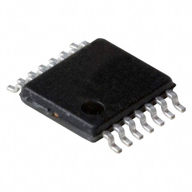
封装信息:SOP14和SSOP14两种封装形式。
NJM339CV-TE1 价格&库存

很抱歉,暂时无法提供与“NJM339CV-TE1”相匹配的价格&库存,您可以联系我们找货

免费人工找货