NJM390A/NJM391A
Low power single voltage comparator
Features
• Wide single supply voltage range or dual supplies
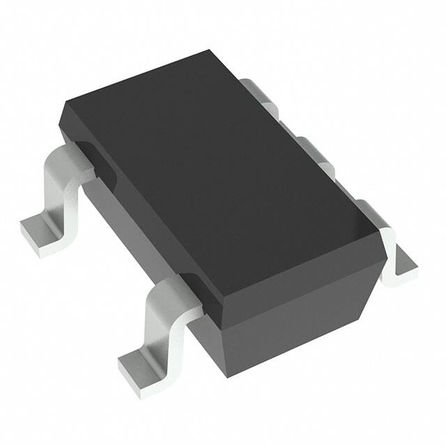
NJM390AF, NJM391AF
( SOT-23-5 )
+2V to +36V or ±1V to ±18V
+
• Very low supply current: 0.3mA typ. at Vcc =5V
• Low input bias current: 20nA typ.
NJM390AF3, NJM391AF3
( SC88A )
• Low input offset current: 0.5nA typ.
• Low input offset voltage: 0.5mV typ.
3mV max.
• Input common-mode voltage range includes ground
NJM391AKG1
( DFN6-G1 (ESON6-G1) )
• Low output saturation voltage: 80mV typ. (Isink = 4mA)
• Differential input voltage range equal to the supply voltage
Pin connections
• TTL, DTL, ECL, MOS, CMOS compatible outputs
• Internal ESD protection
Human body model (HBM) ±2000V typ.
Description
NJM390AF, NJM390AF3
The NJM390A/NJM391A are single comparator designed specifically to
operate from a single supply over a wide range of voltages. Operation from split
power supplies is also possible.
The NJM390A/391A also have a unique characteristic in that the input
common-mode voltage range includes ground even though operated from a
single power supply voltage.
NJM391AF, NJM391AF3
(Top View)
VCC+
N.C.
VCC-
Exposed
Pad on
Underside
Output
1
Schematic diagram
Inverting Input
Non-inverting Input
NJM391AKG1(*)
(*)Connect to exposed pad to VCC-
(*)Connect to exposed pad to V-
Figure 1. Schematic diagram
VCC
(*)Exposed pad はV- に接続ください。
(*)Exposed pad は V- に接続ください。
+
10μA
80μA
10μA
80μA
Output
Vo
Non-Inverting
Non-inverting
Input
Input
Inverting
inverting
Input
Input
VCC
Ver.00
-
-1-
�NJM390A/NJM391A
2
Absolute maximum ratings and operating conditions
Table1. Absolute maximum ratings
Symbol
Parameter
+
-
VCC
Supply voltage(VCC - VCC )
VID
Differential input voltage
VIN
Input voltage
VO
(Tamb=25ºC)
(1)
(2)
Unit
36
V
±36
V
Vcc- -0.3 to Vcc- +36
V
Vcc -0.3 to Vcc +36
V
-
Output short-circuit to VCC
Infinite
-
Tstg
Storage temperature range
-65 to +150
°C
Tj
Output Terminal Input Voltage
Value
- (3)
-
-
Maximum junction temperature
150
(5)
SOT-23-5 :480 ,
(5)
SC88A
:360 ,
PD
Power Dissipation
(7)
DFN6-G1 :330 ,
(5)
SOT-23-5 :260 ,
(4)
(5)
θja
thermal resistance junction to ambient
SC88A
:355 ,
(7)
DFN6-G1 :385 ,
(5)
SOT-23-5 :68 ,
(5)
(4)
SC88A
:91 ,
ψjt
thermal resistance junction to top surface of IC package
(7)
DFN6-G1 :65 ,
+
1. Input voltage is the voltage should be allowed to apply to the input terminal independent of the magnitude of VCC .
+
2. Output voltage is the voltage should be allowed to apply to the output terminal independent of the magnitude of VCC .
°C
(6)
650
(6)
490
(8)
1200
(6)
195
(6)
260
(8)
110
(6)
58
(6)
74
(8)
26
mW
°C /W
°C /W
3. Short-circuits from the output to VCC+ can cause excessive heating and potential destruction.
4. Short-circuit can cause excessive heating and destructive dissipation. Values are typical.
5. EIA/JEDEC STANDARD Test board (76.2 x 114.3 x 1.6mm, 2layers, FR-4) mounting
6. EIA/JEDEC STANDARD Test board (76.2 x 114.3 x 1.6mm, 4layers, FR-4) mounting
7. Mounted on glass epoxy board. (101.5×114.5×1.6mm: based on EIA/JEDEC standard, 2Layers FR-4, with Exposed Pad)
8. Mounted on glass epoxy board. (101.5×114.5×1.6mm: based on EIA/JEDEC standard, 4Layers FR-4, with Exposed Pad)
*For 4Layers: Applying 99.5×99.5mm inner Cu area and a thermal via hole to a board based on JEDEC standard JESD51-5
Table2. Operating conditions
Symbol
VCC
Parameter
+
-
Supply voltage (VCC - VCC )
Tamb =25ºC (unless otherwise specified)
Value
Unit
2 to 36
V
+
Common mode input voltage range (VCC =30V)
Vicm
0 ºC ≤ Tamb ≤ 70 ºC
Toper
+
Tamb = 25℃
0 to VCC -1.5
(5)
Operating free-air temperature range
V
+
0 to VCC -2.0
-40 to +125
°C
.
-2-
Ver.00
�NJM390A/NJM391A
3
Electrical characteristics
Table3. VCC+ = +5V, VCC- = 0V, Tamb = 25˚C (unless otherwise specified)
Symbol
Parameter
Input offset voltage
Vio
Min.
Typ.
Max.
Unit
‐
0.5
3
mV
‐
‐
5
‐
‐
0.5
‐
50
150
‐
20
250
‐
‐
400
50
200
‐
V/mV
‐
0.3
0.5
mA
‐
0.4
1.2
‐
‐
VCC
V
‐
80
400
mV
‐
‐
700
‐
0.1
‐
nA
‐
‐
1
μA
6
16
‐
mA
‐
1.3
‐
μs
‐
250
‐
ns
(1)
Tamb = 25℃
0 ºC ≤ Tamb ≤ 70 ºC
(5)
Input offset current
Iio
Tamb = 25℃
0 ºC ≤ Tamb ≤ 70 ºC
Input bias current
Iib
nA
(2)
Tamb = 25℃
0 ºC ≤ Tamb ≤ 70 ºC
Avd
(5)
(5)
Large signal voltage gain
+
VCC = 15V, RL=15kΩ, Vo = 1V to 11V
nA
Supply current (all comparators)
ICC
+
VCC = +5V, no load
+
VCC = +30V, no load
Vid
Differential input voltage
(3)
+
Low level output voltage(Vid = -1V, Isink = 4mA)
VOL
Tamb = 25℃
0 ºC ≤ Tamb ≤ 70 ºC
(5)
+
High level output current (VCC = Vo = 30V, Vid = 1V)
IOH
Tamb = 25℃
0 ºC ≤ Tamb ≤ 70 ºC
Isink
tre
(5)
Output sink current,Vid = 1V, Vo = 1.5V
Response Time
(4)
+
RL = 5.1kΩ connected to VCC
Large Signal Response Time
trel
+
RL = 5.1kΩ connected to VCC
el = TTL, V(ref) = +1.4V
1. At output switch point, Vo = 1.4V, RS = 0 with VCC+ from 5V to 30V, and over the full common-mode range (0V to VCC+ - 1.5V).
2. The direction of the input current is out of the IC due to the PNP input stage.
3. Positive excursions of input voltage may exceed the power supply level. As long as the other voltage remains within the common-mode range, the
comparator will provide a proper output state. The low input voltage must not be less than –0.3V (or 0.3V below the negative power supply, if used).
4. The response time specified is for a 100mV input step with 5mV overdrive.
5. This parameter is not 100% test.
Ver.00
-3-
�NJM390A/NJM391A
■ TYPICAL CHARACTERISTICS
Supply Current vs. Supply Voltage
Input Bias Current vs. Temperature
VCC- =0V, VCOM=0V, VO=OPEN
1
0.9
80
Ta=25ºC
0.7
Ta=-40ºC
0.6
0.5
0.4
0.3
0.2
0.1
60
Input Bias Current [nA]
Supply Current [mA]
0.8
20
0
-20
-40
VCC+=2V
-80
-100
5
10 15 20 25 30
Supply Voltage VCC+ [V]
35
40
-75 -50 -25
Input Offset Voltage vs. Supply Voltage
3
Ta=25ºC
Input Offset Voltage [mV]
2
1
Ta=-40ºC
0
-1
0 25 50 75 100 125 150
Temperature [ºC]
Input Offset Voltage vs. Temperature
VCC- =0V, VCOM=0V, Vout=1.4V, RL=15kΩ
3
Input Offset Voltage [mV]
VCC+=5V
-60
Ta=125ºC
0
Ta=125ºC
VCC- =0V, VCOM=0V, Vout=1.4V, RL=15kΩ
2
1
VCC+=5V
VCC+=30V
0
-1
VCC+=2V
-2
-2
-3
-3
0
5
10 15 20 25 30
Supply Voltage VCC+ [V]
35
40
-75 -50 -25
Input Offset Voltage
vs. Common-Mode Input Voltage
160
Open-Loop Voltage Gain [dB]
3
2
1
Ta=25ºC
Ta=-40ºC
0 25 50 75 100 125 150
Temperature [ºC]
Large signal voltage gain vs. Temperature
VCC+=30V, VCC- =0V, Vout=1.4V, RL=15kΩ
Input Offset Voltage [mV]
VCC+=30V
40
0
0
-1
Ta=125ºC
-2
VCC+=15V, VCC- =0V, VCOM=1.4V, RL=15kΩ
140
120
100
80
60
40
20
0
-3
-5
-4-
VCC- =0V, VCOM=0V
100
0
5
10
15
20
25
Common-Mode Input Voltage [V]
30
-75 -50 -25
0 25 50 75 100 125 150
Temperature [ºC]
Ver.00
�NJM390A/NJM391A
■ TYPICAL CHARACTERISTICS
Output Saturation Voltage
vs. Supply Voltage
Output Saturation Voltage [mV]
300
Output Saturation Voltage
vs. Output Sink Current
Ta=25ºC
250
ISINK=10mA
200
150
ISINK=6mA
100
ISINK=4mA
50
ISINK=2mA
5
1
Ta=125ºC
Ta=-40ºC
0.01
10 15 20 25 30
Supply Voltage VCC+ [V]
35
0.1
40
Response Time [μs]
0.8
0.7
0.6
Rise
0.5
Fall
0.4
0.3
0.2
0.1
100
600
VCC+=5V, VCC- =0V, ov=100mV, RL=5.1kΩ
500
400
300
Rise
200
Fall
100
0
0
-75 -50 -25
Ver.00
Output Signal Rising/Falling Time [ns]
VCC+=5V, VCC- =0V, Ov=100mV, RL=5.1kΩ
0.9
1
10
Output Sink Current [mA]
Output Signal Rising/Falling Time
vs. Temperature
Response Time vs. Temperature
1
Ta=25ºC
0.1
0.001
0
0
VCC+=5V, VCC- =0V, VID=-1V
10
Output Saturation Voltage [V]
VCC- =0V,
0 25 50 75 100 125 150
Temperature [ºC]
-75 -50 -25
0 25 50 75 100 125 150
Temperature [ºC]
-5-
�NJM390A/NJM391A
■ TYPICAL CHARACTERISTICS
Response Time
Response Time
ov=5mV
0.6
0.9
4
0.8
3
0.7
2
ov=20mV
0.5
1
ov=100mV
0.4
0
0.3
-1
0.2
-2
0.1
6
5
4
ov=5mV
3
Output
ov=20mV
0.6
2
ov=100mV
0.5
1
0.4
0
0.3
-1
0.2
-2
Input
-3
0.1
-3
0
-4
0
-4
-0.1
-5
-0.1
-5
-0.2
-6
-0.2
Input
-1
0
1
2
3
-6
-1
0
0.25μs/div
CL=47pF
CL=100pF
Input
-1
0
1
0.25μs/div
-6-
2
3
Input Voltage [V]
CL=0pF
Output
2
3
Response Time
6
5
4
3
2
1
0
-1
-2
-3
-4
-5
-6
-7
OutputVoltage [V]
Input Voltage [V]
Response Time
VCC+=5V, VCC- =0V, RL=5.1kΩ, VREF=1.4V, Ta=25ºC
12
11
10
9
8
7
6
5
4
3
2
1
0
-1
1
0.25μs/div
VCC+=5V, VCC- =0V, RL=5.1kΩ, VREF=1.4V, Ta=25ºC
12
11
10
9
8
7
6
5
4
3
2
1
0
-1
Output
6
5
4
3
2
1
0
-1
-2
-3
-4
-5
-6
-7
CL=0pF
CL=47pF
CL=100pF
Input
-1
0
1
0.25μs/div
2
OutputVoltage [V]
Input Voltage [V]
0.7
1
5
VCC+=5V, V- =0V, RL=5.1kΩ, VREF=0V, CL=0PF, Ta=25
Output Voltage [V]
Output
0.8
6
Input Voltage [V]
1
0.9
Output Voltage [V]
VCC+=5V, VCC- =0V, RL=5.1kΩ, VREF=0V, CL=0PF, Ta=25ºC
3
Ver.00
�NJM390A/NJM391A
■PACKAGE OUTLINE UNIT : mm
SOT-23-5
2.9±0.2
0°~15°
4
2
1
0.6
2.8±0.2
+0.2
1.6 - 0.1
5
0.2MIN
1.9±0.2
3
0.95±0.1
+0.1
0.1-0.03
0.1MAX
1.1±0.1
0.6MAX
0.4±0.1
0.1
SC-88A
0.425±0.2
2.0±0.2
1.3±0.2
2
(0.245)
3
0.425±0.2
+0.1
0.23-0.05
0-10°
0.05±0.05
0.9±0.1
+0.2
0.2- 0.1
0.65±0.07
+0.05
0.95- 0.15
1
2.1±0.2
4
1.25±0.1
5
+0.1
0.13-0.03
Ver.00
-7-
�NJM390A/NJM391A
■PACKAGE OUTLINE UNIT : mm
DFN6-G1 (ESON6-G1)
[CAUTION]
The specifications on this databook are only
given for information , without any guarantee
as regards either mistakes or omissions. The
application circuits in this databook are
described only to show representative usages
of the product and not intended for the
guarantee or permission of any right including
the industrial rights.
-8-
Ver.00
�