Advanced Science And Novel Technology Company, Inc.
2790 Skypark Drive Suite 112, Torrance, CA 90505
Offices: 310-530-9400 / Fax: 310-530-9402
www.adsantec.com
ASNT7123-KMA
16GS/s, 4-bit Flash Analog-to-Digital Converter with HS Outputs
20GHz analog input bandwidth
Selectable clocking mode: external high-speed clock or internal PLL with external reference clock
Broadband operation in external clocking mode: DC-16GS/s
On-chip PLL with a central frequency of 10GHz
Selectable on-chip PRBS 215-1 generator for output data scrambling
Differential CML input clock buffer and output data and clock buffers
Differential linear data input buffer
LVDS input reference clock buffer
Selectable on-chip digital-to-analog converter for self-testing
Single +3.5V power supply
Power consumption: 4.62W
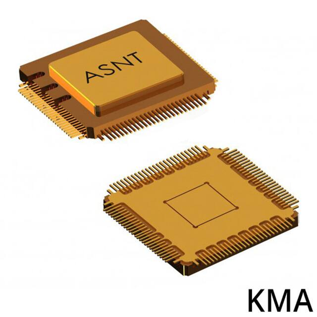
Custom 100-pin metal-ceramic package
vee 75
vee 74
nc 73
nc 72
vcc 71
nc 70
nc 69
vcc 68
nc 67
nc 66
vcc 65
nc 64
nc 63
vcc 62
rstn 61
rstp 60
vcc 59
vee 58
odn 57
odp 56
vcc 55
n/c 54
n/c 53
vcc 52
vee 51
Rev. 1.4.2
ASNT7122
ASNT7123
Power
consum
vee 50
vrefcrl 49
vlsbcrl 48
ondac 47
nc 46
onprbs 45
vcc 44
vee 43
vee 42
vcc 41
dp 40
dn 39
vcc 38
vee 37
vee 36
vcc 35
cep 34
cen 33
vcc 32
vee 31
vee 30
vcc 29
crp 28
crn 27
vcc 26
1 vee
2 vee
3 nc
4 nc
5 vcc
6 chop
7 chon
8 vcc
9 nc
10 nc
11 vcc
12 nc
13 nc
14 vcc
15 vee
16 ondata
17 nc
18 nc
19 lol
20 ftr
21 vee
22 ceoff
23 nc
24 nc
cpcsel
25 vcc
76 vcc
77 nc
78 nc
79 vcc
80 q03p
81 q03n
82 vcc
83 nc
84 nc
85 vcc
86 q02p
87 q02n
88 vcc
89 q01p
90 q01n
91 vcc
92 nc
93 nc
94 vcc
95 q00p
96 q00n
97 vcc
98 nc
99 nc
100 vcc
1
February 2020
�Advanced Science And Novel Technology Company, Inc.
2790 Skypark Drive Suite 112, Torrance, CA 90505
Offices: 310-530-9400 / Fax: 310-530-9402
www.adsantec.com
DESCRIPTION
ondac
DAC
ondata
vrefcrl
vlsbcrl
dp/dn
rstp/n
onprbs
ftr
lol
crp/crn
cep/cen
LIB 15
4-bit
TTB
Flash 15
Encoder
ADC
LOB
SCR
x4
odp/odn
OB
CMLx4
q00p/q00n
q01p/q01n
q02p/q02n
q03p/q03n
OB
CML
chop/chon
PRBS
CMU &
Divider
ceoff
Fig. 1. Functional Block Diagram
The ASNT7123-KMA is a 4-bit flash analog to digital converter (ADC) featuring a high sampling rate,
and wide analog front-end bandwidth. The ADC system shown in Fig. 1 includes a linear input buffer
(LIB) with tree-type architecture, and a CML-type input interface with internal 50Ohm single-ended
terminations to vcc. The buffer delivers 15 matching copies of the input analog data signal dp/dn to the
4-bit flash ADC. The ADC creates 15 samples of the input data in thermometer code, which are then
converted by a thermometer-to-binary encoder (TTB Encoder) into 4-bit binary words with a data rate f.
The ADC thresholds are controlled by signals vrefcrl and vlsbcrl.
The encoded data is processed by a scrambler (SCRx4) where it is mixed with a 215-1 PRBS signal
provided by an internal PRBS generator (PRBS). The scrambled data is delivered to a 4-bit differential
CML output interface (OB CMLx4, pins q00p/q00n, q01p/q01n, q02p/q02n, q03p/q03n). The PRBS
generator can be preset to a certain initial state by the differential external signal rstp/rstn, or completely
disabled by control signal onprbs. When disabled, the generator allows data to pass unchanged through
the scrambler. It is also possible to disable the data by using control signal ondata, and pass the PRBS
signal to the outputs. An optional digital-to-analog converter (DAC) with an output signal odp/odn can
be used to control the ADC’s operation. It is enabled by control signal ondac.
All operations are synchronized by the internal clock multiplication unit (CMU) based on a PLL (phaselocked loop) with an integrated divider, and an external loop filter connected to pin ftr. The block can
operate in two different modes, and is controlled by signal ceoff: they can either be clock multiplication
(PLL is on, a reference clock is applied to pins crp/crn), or clock division (PLL is off, an external highspeed clock is applied to pins cep/cen). In both modes, the divider generates internal clock signals
divided by 2, 4, 8, and 16. The generated divided clocks are sent to different internal blocks. A PLL lock
control output lol is also provided.
Rev. 1.4.2
2
February 2020
�Advanced Science And Novel Technology Company, Inc.
2790 Skypark Drive Suite 112, Torrance, CA 90505
Offices: 310-530-9400 / Fax: 310-530-9402
www.adsantec.com
The part operates from a single +3.5V power supply. All external control signals are compatible with the
2.5V CMOS interface.
Linear Input Buffer (LIB)
The system includes a linear input buffer (LIB) with a tree-type architecture that delivers 15 matching
copies of the wide-band input differential analog data signal dp/dn to the 4-bit flash section. Symmetry is
closely followed in both schematic, and layout to ensure minimal aperture jitter.
Clock Multiplication Unit (CMU) & Divider
The PLL-based CMU with its external loop filter connected to pin ftr as shown in Fig. 2 can operate in
two different modes. In the first “clock multiplication” mode (ceoff=”1”, default), the CMU multiplies
the external reference clock crp/crn with a speed of f/16 by means of a PLL with a central frequency of f
and a wide tuning range of the internal VCO (voltage-controlled oscillator). The generated clock is
processed by the divider in order to generate internal clock signals divided by 2, 4, 8, and 16.
100Ohm
To pin 20 (ftr)
1nF
vee
Fig. 2. Recommended External Loop Filter Schematic
In the second “clock division” mode (ceoff=”0”), the PLL is disabled and the internal clocks are
generated from the external high-speed clock inputs cep/cen.
HS External Clock Input Buffer
The high-speed external clock input buffer can accept high-speed clock signals at its differential CML
input port cep/cen. It can also accept a single-ended signal with AC or DC termination. In case of AC
termination, the unused pin should be also AC terminated with a 50Ohm load. In case of DC termination,
a threshold voltage must be applied to the unused pin. Differential input signaling must be used for input
clock frequencies above 14GHz. The buffer can handle a wide range of input signal amplitudes. The
buffer utilizes on-chip single-ended termination of 50Ohm to vcc for each input line.
LS Reference Clock Input Buffer
The low-speed reference clock input buffer is a proprietary LVDS buffer with internal 100Ohm
differential termination between its inputs crp/crn. The buffer exceeds the requirements of standards
IEEE Std. 1596.3-1996 and ANSI/TIA/EIA-644-1995. It is designed to accept differential signals with
amplitudes above 100mV peak-to-peak (p-p), a wide range of DC common mode voltages, and AC
common mode noise with a frequency up to 5MHz and voltage levels ranging from 0 to 2.4V.
4-bit Flash Analog to Digital Converter (ADC) with Encoder
This block samples the incoming analog data with the clock signal provided by the CMU in order to
generate a 4-bit output digital signal (Bit 0 – Bit 3) with MSB corresponding to Bit 3. The threshold
voltages (Vth 1 - Vth 15) of the ADC can be adjusted through analog signals vrefcrl and vlsbcrl as shown in
Table 1. As can be seen, vrefcrl shifts the DC levels of all the threshold voltages simultaneously by the
same amount in relation to vcc and vlsbcrl alters the voltage range of the least significant bit (LSB) while
also shifting the DC levels.
Rev. 1.4.2
3
February 2020
�Advanced Science And Novel Technology Company, Inc.
2790 Skypark Drive Suite 112, Torrance, CA 90505
Offices: 310-530-9400 / Fax: 310-530-9402
www.adsantec.com
Table 1. Simulated ADC Threshold Control States
vrefcrl. mV
min (vcc – 960)
min (vcc – 960)
max (vcc)
max (vcc)
vlsbcrl. mV
Vth 15, mV Vth 8, mV Vth 1, mV Vth (X+1) – Vth X, mV
min (vcc – 700) vcc-35
vcc-54
vcc-73
2.7
max (vcc – 260) vcc-345 vcc-751 vcc-1157
58
min (vcc – 700) vcc-355 vcc-361 vcc-366
0.8
max (vcc – 260) vcc-665 vcc-1058 vcc-1450
56
If no external voltages are applied to vrefcrl and vlsbcrl, it is recommended to have both pins ACterminated by 50Ohm resistors to vee through DC blocks! The corresponding default states are
vrefcrl=vlsbcrl=vcc-0.48V.
PRBS Generator (PRBS)
The on-chip selectable generator provides a full 32-kbit long pseudo-random binary sequence (PRBS)
signal according to the polynomial (x15 + x14 + 1), where xD represents a delay of D clock cycles. This is
implemented as a linear feedback shift register (LFSR) in which the outputs of the fifteenth and fourteenth
flip-flops are combined together by an XOR function and provided as an input to the first flip-flop of the
register. The block is activated by the external 2.5V CMOS signal onprbs (onprbs=”0” – default state –
PRBS generator off, onprbs=”1” – PRBS generator on). The same signal sets the PRBS output to logic
“0” state that is required for the transparency of the following scrambler block SCRx4.
The LSFR-based PRBS generator produces 32,767 binary states, excluding the “all zeros” state that is
illegal for the XOR-based configuration. To eliminate this state that locks the LFSR and prevents PRBS
generation, an asynchronous external CML reset signal (rstp/rstn) should be applied to the circuit. When
the reset is asserted, LSFR is set to the all-“1” state that is enough for the activation of PRBS generation.
When the preset is released, the block delivers four copies of the same signal to the scrambler.
Scrambler (SCRx4)
The scrambler SCHx4 consists of four symmetrical XOR gates that mix four signals delivered by the
encoder with the generated PRBS signal. To ensure reliable operation of the block, all signals are retimed
by D-type flip-flops before and after the scrambling. The scrambler can be configured to pass either
scrambled data (ondata=”1”, default), or PRBS signal only (ondata=”0”).
Digital to Analog Converter (DAC)
A DAC block is included to perform a quick test of the ADC’s functionality. When activated by external
control signal (ondac=”1”), it converts the digital data into a step-wise copy of the input signal that is
sent to the output odp/odn through a linear differential output buffer LOB. The circuit is not consuming
any power when disabled (ondac=”0”, default).
CML Data Output Buffers (OB CMLx4)
The data output buffers (OB CMLx4) receive four high-speed data signals from the scrambler and convert
them into differential CML output signals q00p/q00n, q01p/q01n, q02p/q02n, and q03p/q03n. Each
buffer utilizes internal single-ended 50Ohm loads to vcc and requires single-ended 50Ohm external
termination. The termination resistors can be connected from each output directly to vcc, or through DC
blocks to vee. The output drivers of the buffers are slightly linearized to deliver optimal eye shape.
Rev. 1.4.2
4
February 2020
�Advanced Science And Novel Technology Company, Inc.
2790 Skypark Drive Suite 112, Torrance, CA 90505
Offices: 310-530-9400 / Fax: 310-530-9402
www.adsantec.com
CML Clock Output Buffer (OB CML)
The high-speed clock output buffer (OB CML) is a replica of one data output buffer.
TERMINAL FUNCTIONS
Pin
Pin
Pin
Pin
Termination
# name
type
function
or connection
1
vee
supply voltage
negative power supply
GND
2
vee
supply voltage
negative power supply
GND
3
n/c
not used
4
n/c
not used
5
vcc
supply voltage
positive power supply
6
chop
CML output
HS output clock, direct
50Ohm to vcc
7
chon
CML output
HS output clock, inverted
50Ohm to vcc
8
vcc
supply voltage
positive power supply
9
n/c
not used
10
n/c
not used
11
vcc
supply voltage
positive power supply
12
n/c
not used
13
n/c
not used
14
vcc
supply voltage
positive power supply
15
vee
supply voltage
negative power supply
GND
16 ondata CMOS input
Data to output on/off
1MOhm to 2.5V
17
n/c
not used
18
n/c
not used
19
lol
CMOS output
PLL no-lock indicator
20
ftr
External filter connection
21
vee
supply voltage
negative power supply
GND
22 ceoff
CMOS input Clock multiplication/division mode 1MOhm to 2.5V
23
n/c
not used
24
n/c
not used
25
vcc
supply voltage
positive power supply
26
vcc
supply voltage
positive power supply
27
crn
LVDS
LS reference input clock, direct
100Ohm
input
between
pins
28
crp
LS reference input clock, inverted
29
vcc
supply voltage
positive power supply
30
vee
supply voltage
negative power supply
GND
31
vee
supply voltage
negative power supply
GND
32
vcc
supply voltage
positive power supply
33
cen
CML input
HS input clock, direct
50Ohm to vcc
34
cep
CML input
HS input clock, inverted
50Ohm to vcc
35
vcc
supply voltage
positive power supply
36
vee
supply voltage
negative power supply
GND
37
vee
supply voltage
negative power supply
GND
38
vcc
supply voltage
positive power supply
Rev. 1.4.2
5
February 2020
�Advanced Science And Novel Technology Company, Inc.
2790 Skypark Drive Suite 112, Torrance, CA 90505
Offices: 310-530-9400 / Fax: 310-530-9402
www.adsantec.com
Pin
Pin
Pin
# name
type
39
dn
Analog input
40
dp
Analog input
41
vcc
supply voltage
42
vee
supply voltage
43
vee
supply voltage
44
vcc
supply voltage
45 onprbs CMOS input
46
n/c
47 ondac
CMOS input
48 vlsbcrl Analog voltage
49
50
51
52
53
54
55
56
57
58
59
60
61
62
63
64
65
66
67
68
69
70
71
72
73
74
75
76
77
78
79
Rev. 1.4.2
Pin
function
HS input data, direct
HS input data, inverted
positive power supply
negative power supply
negative power supply
positive power supply
PRBS enable/disable
not used
DAC enable/disable
ADC threshold
voltages controls
Termination
or connection
50Ohm to vcc
50Ohm to vcc
GND
GND
1MOhm to vee
1MOhm to vee
12KOhm to vcc
vrefcrl Analog voltage
12KOhm to vcc
vee
supply voltage
negative power supply
GND
vee
supply voltage
negative power supply
GND
vcc
supply voltage
positive power supply
n/c
not used
n/c
not used
vcc
supply voltage
positive power supply
odp
Analog output
DAC output signal, direct
50Ohm to vcc
odn
Analog output
DAC output signal, inverted
50Ohm to vcc
vee
supply voltage
negative power supply
GND
vcc
supply voltage
positive power supply
rstp
CML input
HS PRBS reset signal, direct
50Ohm to vcc
rstn
CML input
HS PRBS reset signal, inverted 50Ohm to vcc
vcc
supply voltage
positive power supply
n/c
not used
n/c
not used
vcc
supply voltage
positive power supply
n/c
not used
n/c
not used
vcc
supply voltage
positive power supply
n/c
not used
n/c
not used
vcc
supply voltage
positive power supply
n/c
not used
n/c
not used
vee
supply voltage
negative power supply
GND
vee
supply voltage
negative power supply
GND
vcc
supply voltage
positive power supply
n/c
not used
n/c
not used
vcc
supply voltage
positive power supply
6
February 2020
�Advanced Science And Novel Technology Company, Inc.
2790 Skypark Drive Suite 112, Torrance, CA 90505
Offices: 310-530-9400 / Fax: 310-530-9402
www.adsantec.com
Pin Pin
Pin
Pin
# name
type
function
80 q03p
CML output
Output data Bit 3, direct
81 q03n
CML output Output data Bit 3, inverted
82
vcc supply voltage
positive power supply
83
n/c
not used
84
n/c
not used
85
vcc supply voltage
positive power supply
86 q02p
CML output
Output data Bit 2, direct
87 q02n
CML output Output data Bit 2, inverted
88
vcc supply voltage
positive power supply
89 q01p
CML output
Output data Bit 1, direct
90 q01n
CML output Output data Bit 1, inverted
91
vcc supply voltage
positive power supply
92
n/c
not used
93
n/c
not used
94
vcc supply voltage
positive power supply
95 q00p
CML output
Output data Bit 0, direct
96 q00n
CML output Output data Bit 0, inverted
97
vcc supply voltage
positive power supply
98
n/c
not used
99
n/c
not used
100 vcc supply voltage
positive power supply
Termination
or connection
50Ohm to vcc
50Ohm to vcc
50Ohm to vcc
50Ohm to vcc
50Ohm to vcc
50Ohm to vcc
50Ohm to vcc
50Ohm to vcc
ABSOLUTE MAXIMUM RATINGS
Caution: Exceeding the absolute maximum ratings presented in Table 2 may cause damage to this product
and/or lead to reduced reliability. Functional performance is specified over the recommended operating
conditions for power supply and temperature only. AC and DC device characteristics at or beyond the
absolute maximum ratings are not assumed or implied. All min and max voltage limits are referenced to
ground (vee).
Table 2. Absolute Maximum Ratings
Parameter
Supply Voltage (vcc)
Power Consumption
RF Input Voltage Swing (SE)
Case Temperature
Storage Temperature
Operational Humidity
Storage Humidity
Rev. 1.4.2
Min
-40
10
10
7
Max
4.0
5.5
1.4
+100
+100
98
98
Units
V
W
V
ºC
ºC
%
%
February 2020
�Advanced Science And Novel Technology Company, Inc.
2790 Skypark Drive Suite 112, Torrance, CA 90505
Offices: 310-530-9400 / Fax: 310-530-9402
www.adsantec.com
ELECTRICAL CHARACTERISTICS
PARAMETER
TYP MAX
UNIT
COMMENTS
General Parameters
3. 4
3.5
3.6
V
±3%
vcc
0.0
V
External ground
vee
Ivcc
1320
mA
With PRBS and DAC enabled
Power consumption
4.62
W
With PRBS enabled
Junction temperature
-25
50
125
°C
Analog Input Data (dp/dn)
Bandwidth
0.0
20
GHz
CM Level
vcc-0.8
vcc
V
Must match for both inputs
Linearity range
±110
mV
Differential or SE, p-p
HS Input Clock (cep/cen)
Frequency
DC
16
GHz
Swing
0.2
1.0
V
Differential or SE, p-p
CM Voltage Level
vcc-0.8
vcc
V
Must match for both inputs
Duty Cycle
40
50
60
%
LS Reference Input Clock (crp/crn)
Frequency
560
688
MHz
1/16 of VCO frequency
CM Level
0.2
vcc
V
Voltage Swing
100
800
mV
Differential
Duty Cycle
40
50
60
%
HS Output Clock and Data (chop/chon, q00p/q00n to q03p/q03n)
Data Rate
DC
16
Gbps
For data signals
Frequency
DC
16
GHz
For clock signals
Logic “1” level
V
vcc
Logic “0” level
vcc-0.6
V
Rise/Fall Times
TBD
ps
20%-80%
DAC Output (odp/odn)
Voltage Swing
250
350
mV
Single-ended. p-p
CM Level
vcc-(voltage swing)/2
V
Analog Control Signals (vrefcrl, vlsbcrl)
Voltage range
V
see Table 1
CML Control Signals (rstp/rstn)
Pulse width
83
ps
1 period of HS clock
Swing
0.2
0.8
V
Differential or SE, p-p
CM Voltage Level
vcc-0.8
vcc
V
Must match for both inputs
CMOS Control Signals (ceoff, ondac, onprbs, ondata)
Logic “1” level
vee+2.3
vee+2.5
V
Logic “0” level
vee+0.2
V
Frequency
3.5
GHz
Rev. 1.4.2
MIN
8
February 2020
�Advanced Science And Novel Technology Company, Inc.
2790 Skypark Drive Suite 112, Torrance, CA 90505
Offices: 310-530-9400 / Fax: 310-530-9402
www.adsantec.com
ELECTRICAL SPECIFICATIONS
Parameter
ENOB (5GS/s)
ENOB (8GS/s)
ENOB (10GS/s)
ENOB (12GS/s)
SFDR (5GS/s)
SFDR (10GS/s)
SINAD (5GS/s)
SINAD (10GS/s)
DNL
INL
Conditions
fin = 3.9GHz
fin = 8.0GHz
fin = 10.0GHz
fin = 12.0GHz
fin = 3.9GHz
fin = 7.8GHz
fin = 3.9GHz
fin = 7.8GHz
Min
Typical
3.39
3.35
3.30
3.26
30.13
28.78
-22.15
-21.19
-0.2
-0.2
Max
0.2
0.2
Units
bits
bits
bits
bits
dBFS
dBFS
dB
dB
lsbs
lsbs
Fig. 3 presents ENOB measured at the sampling rates of 9GSps and 14GSps. The differential input signal
is applied through a coupler or from the outputs of the ADSANTEC’s analog signal splitter ASNT6114.
Fig. 3. ENOB at 9GSps and 14GSps
Rev. 1.4.2
9
February 2020
�Advanced Science And Novel Technology Company, Inc.
2790 Skypark Drive Suite 112, Torrance, CA 90505
Offices: 310-530-9400 / Fax: 310-530-9402
www.adsantec.com
PACKAGE INFORMATION
The chip die is housed in a custom 100-pin CQFP package shown in Fig. 4.
Fig. 4. CQFP 100-Pin Package Drawing (All Dimensions in mm)
Rev. 1.4.2
10
February 2020
�Advanced Science And Novel Technology Company, Inc.
2790 Skypark Drive Suite 112, Torrance, CA 90505
Offices: 310-530-9400 / Fax: 310-530-9402
www.adsantec.com
The package provides a center heat slug located on its back side to be used for heat dissipation.
ADSANTEC recommends for this section to be soldered to the vcc plain, which is power for a positive
supply.
The part’s identification label is ASNT7123-KMA. The first 8 characters of the name before the dash
identify the bare die including general circuit family, fabrication technology, specific circuit type, and part
version while the 3 characters after the dash represent the package’s manufacturer, type, and pin out
count.
This device complies with the Restriction of Hazardous Substances (RoHS) per 2011/65/EU for all ten
substances.
REVISION HISTORY
Revision
1.4.2
1.3.2
1.2.2
1.2.1
1.1.1
1.0.1
0.0.1
Rev. 1.4.2
Date
02-2020
10-2019
07-2019
07-2018
12-2017
12-2017
04-2017
Changes
Updated Package Information
Corrected frequency range for input clock
Updated Letterhead
Added Fig. 3.
Updated electrical specifications
Initial release
Preliminary release
11
February 2020
�