CA3310, CA3310A
UCT
T
PROD
E
T
EM EN
E
L
E PL A C
t
O B SO
R
D
te
E
en r a
ND
port C
O MM E
p
C
u
s
S
E
l
/t
R
a
om c
NO
chnicSheet
ersil.c
TeData
t
r
n
u
.i
o
w
t
or w w
contac
TERSIL
IN
8
8
1-8
®
CMOS, 10-Bit, A/D Converters with
Internal Track and Hold
May 2001
• CMOS Low Power (Typ) . . . . . . . . . . . . . . . . . . . . . 15mW
The ten data outputs feature full high-speed CMOS threestate bus driver capability, and are latched and held through
a full conversion cycle. Separate 8 MSB and 2 LSB enables,
a data ready flag, and conversion start and ready reset
inputs complete the microprocessor interface.
• Single Supply Voltage . . . . . . . . . . . . . . . . . . . . . 3V to 6V
• Conversion Time . . . . . . . . . . . . . . . . . . . . . . . . . . . . 13µs
• Built-In Track and Hold
• Rail-to-Rail Input Range
• Latched Three-state Output Drivers
• Microprocessor-Compatible Control Lines
• Internal or External Clock
Applications
• Fast, No-Droop, Sample and Hold
An internal, adjustable clock is provided and is available as
an output. The clock may also be driven from an external
source.
• Voice Grade Digital Audio
Part Number Information
• µP Controlled Systems
LINEARITY
(INL, DNL)
TEMP.
RANGE
(oC)
CA3310E
±0.75 LSB
-40 to 85
24 Ld PDIP
E24.6
CA3310M
±0.75 LSB
-40 to 85
24 Ld SOIC
M24.3
CA3310AM
±0.5 LSB
-40 to 85
24 Ld SOIC
M24.3
1
PACKAGE
3095.3
Features
The Intersil CA3310 is a fast, low power, 10-bit successive
approximation analog-to-digital converter, with
microprocessor-compatible outputs. It uses only a single 3V
to 6V supply and typically draws just 3mA when operating at
5V. It can accept full rail-to-rail input signals, and features a
built-in track and hold. The track and hold will follow high
bandwidth input signals, as it has only a 100ns (typical) input
time constant.
PART
NUMBER
File Number
PKG.
NO.
• DSP Modems
• Remote Low Power Data Acquisition Systems
Related Literature
• Technical Brief TB363 “Guidelines for Handling and
Processing Moisture Sensitive Surface Mount Devices
(SMDs)”
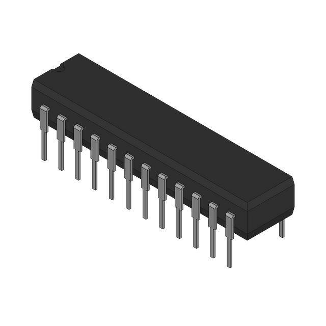
Pinout
CA3310, CA3310A
(PDIP, SOIC)
TOP VIEW
D0 (LSB)
1
24
D1
2
23
VIN
D2
3
22
VREF +
D3
4
21
REXT
D4
5
20
CLK
D5
6
19
STRT
D6
7
18
VREF -
D7
8
17
VAA+
VDD
D8
9
16
VAA-
D9 (MSB)
10
15
OEL
DRDY
11
14
OEM
VSS (GND)
12
13
DRST
CAUTION: These devices are sensitive to electrostatic discharge; follow proper IC Handling Procedures.
1-888-INTERSIL or 321-724-7143 | Intersil (and design) is a registered trademark of Intersil Americas Inc.
Copyright © Intersil Americas Inc. 2002. All Rights Reserved
�CA3310, CA3310A
Functional Block Diagram
STRT
VDD
VSS
ALL
LOGIC
REXT
CLOCK
CONTROL
AND
TIMING
VIN
VREF +
CLK
DRDY
Q
CLK
CLR
DRST
OEM
16C
D9 (MSB)
8C
50ÞΩ
SUBSTRATE
RESISTANCE
D8
4C
D7
2C
D6
VAA +
C
32
C
31
16C
VAA -
8C
10-BIT
SUCCESSIVE
APPROXIMATION
REGISTER
10-BIT
EDGE
TRIGGERED
“D”
LATCH
D5
D4
D3
4C
D2
2C
D1
C
D0 (LSB)
C
OEL
VREF -
2
�CA3310, CA3310A
Typical Application Schematics
+5V SUPPLY
4.7µF
TAN
+
0.1µF CER
A
8
ICL7663S
3 100Ω ±10%
4.5V
1
75V
6
4
D
VDD
VREF +
4.7µF +
TAN
STRT
START CONVERSATION
DRST
RESET FLAG
A
5K
ADJUST
GAIN
VAA +
28.7K
VREF -
5
HIGH BYTE ENABLE
OEL
LOW BYTE ENABLE
CA3310/A
D0 - D9
A
A
A
OEM
OUTPUT DATA
VAA R3
R2
+8V
TO
+15V
100
0.1
A
R1
8
+
VIN
A
7
3
+
2 CA3140
-
-
R4
10K
4
A
CLK
VDD
REXT
VIN
R5
2MHz CLOCK
NC
VSS
UNLESS NOTED,
ALL RESISTORS =
1% METAL FILM,
POTS = 10 TURN, CERMET
47pF
1
D
ADJUST
OFFSET
0.1
-1V
TO
-15V
OPTIONAL
CLAMP
6
5
DATA READY FLAG
DRDY
A
A
D = DIGITAL GROUND
A = ANALOG GROUND
D
100
INPUT RANGE
R1
R2
R3
R4
R5
0V To 2.5V
4.99K
9.09K
OPEN
4.99K
9.09K
0V To 5V
4.99K
4.53K
OPEN
4.99K
4.53K
0V To 10V
10K
4.53K
OPEN
10K
4.53K
-2.5V To +2.5V
4.99K
9.09K
9.09K
4.99K
4.53K
-5V To +5V
10K
9.09K
9.09K
10K
4.53K
3
�CA3310, CA3310A
Absolute Maximum Ratings
Thermal Information
Digital Supply Voltage VDD . . . . . . . . . . . . . . VSS -0.5V to V SS +7V
Analog Supply Voltage (V AA+) . . . . . . . . . . . . . . . . . . . . VDD ±0.5V
Any Other Terminal . . . . . . . . . . . . . . . . VSS -0.5V to VDD + 0.5V
DC Input Current or Output (Protection Diode)
Current . . . . . . . . . . . . . . . . . . . . . . . . . . . . . . . . . . . . . . . . ±20mA
DC Output Drain Current, per Output . . . . . . . . . . . . . . . . . . ±35mA
Total DC Supply or Ground Current. . . . . . . . . . . . . . . . . . . . ±70mA
Thermal Resistance (Typical, Note 1)
Operating Conditions
θJA ( oC/W)
PDIP Package . . . . . . . . . . . . . . . . . . . . . . . . . . . . .
60
SOIC Package . . . . . . . . . . . . . . . . . . . . . . . . . . . . .
75
Maximum Junction Temperature
Plastic Packages . . . . . . . . . . . . . . . . . . . . . . . . . . . . . . . . . 150oC
Maximum Storage Temperature (TSTG) . . . . . . . . . -65oC to 150oC
Maximum Lead Temperature (Soldering 10s) . . . . . . . . . . . . 300oC
(SOIC - Lead Tips Only)
Temperature Range (TA) . . . . . . . . . . . . . . . . . . . . . . -40oC to 85oC
CAUTION: Stresses above those listed in “Absolute Maximum Ratings” may cause permanent damage to the device. This is a stress only rating and operation of the
device at these or any other conditions above those indicated in the operational sections of this specification is not implied.
NOTE:
1. θJA is measured with the component mounted on a low effective thermal conductivity test board in free air. See Tech Brief TB379 for details.
TA = 25×oC, VDD = VAA+ = 5V, VREF + = 4.608V, VSS = VAA- = VREF - = GND, CLK = External 1MHz, Unless
Otherwise Specified
Electrical Specifications
PARAMETER
TEST CONDITIONS
MIN
TYP
MAX
UNITS
ACCURACY (See Text For Definitions)
Resolution
Differential Linearity Error
Integral Linearity Error
Gain Error
Offset Error
10
-
-
Bits
CA3310
-
±0.5
±0.75
LSB
CA3310A
-
±0.25
±0.5
LSB
CA3310
-
±0.5
±0.75
LSB
CA3310A
-
±0.25
±0.5
LSB
CA3310
-
±0.25
±0.5
LSB
CA3310A
-
-
±0.25
LSB
CA3310
-
±0.25
±0.5
LSB
CA3310A
-
-
±0.25
LSB
-
330
-
Ω
ANALOG INPUT
Input Resistance
In Series with Input Sample Capacitors
Input Capacitance
During Sample State
-
300
-
pF
Input Capacitance
During Hold State
-
20
-
pF
Input Current
At VIN = VREF + = 5V
-
-
+300
µA
At VIN = VREF - = 0V
-
-
-100
µA
Static Input Current
STRT = V+, CLK = V+
At VIN = VREF + = 5V
-
-
1
µA
-
-
-1
µA
(Note 3)
VREF - +1
-
VDD +0.3
V
Input - Full-Scale Range
(Note 3)
V SS -0.3
-
VREF + -1
V
Input Bandwidth
From Input RC Time Constant
-
1.5
-
MHz
At VIN = VREF - = 0V
Input + Full-Scale Range
DIGITAL INPUTS DRST, OEL, OEM, STRT, CLK
High-Level Input Voltage
Over V DD = 3V to 6V (Note 3)
70
-
-
% of VDD
Low-Level Input Voltage
Over V DD = 3V to 6V (Note 3)
-
-
30
% of VDD
Input Leakage Current
Except CLK
-
-
±1
µA
Input Capacitance
(Note 3)
-
-
10
pF
Input Current
CLK Only (Note 3)
-
-
±400
µA
High-Level Output Voltage
ISOURCE = -4mA
4.6
-
-
V
Low-Level Output Voltage
ISINK = 6mA
-
-
0.4
V
Three-State Leakage
Except DRDY
-
-
±1
µA
Output Capacitance
Except DRDY (Note 3)
-
-
20
pF
DIGITAL OUTPUTS D0 - D9, DRDY
4
�CA3310, CA3310A
TA = 25×oC, VDD = VAA+ = 5V, VREF + = 4.608V, VSS = VAA- = VREF - = GND, CLK = External 1MHz, Unless
Otherwise Specified (Continued)
Electrical Specifications
PARAMETER
TEST CONDITIONS
MIN
TYP
MAX
UNITS
CLK OUTPUT
High-Level Output Voltage
ISOURCE = 100µA (Note 3)
4
-
-
V
Low-Level Output Voltage
ISlNK = 100µA (Note 3)
-
-
1
V
200
300
400
kHz
600
800
1000
kHz
-
4
2
MHz
TIMING
Internal, CLK and R EXT Open
Clock Frequency
Internal, CLK Shorted to REXT
External, Applied to CLK (Note 3)
(Max)
100
10
-
kHz
Clock Pulse Width, tLOW , tHIGH
External, Applied to CLK:
See Figure 1 (Note 3)
(Min)
100
-
-
ns
Conversion Time
Internal, CLK Shorted to REXT
13
-
-
µs
Aperture Delay, tD APR
See Figure 1
-
100
-
ns
Clock to Data Ready Delay, tD1 DRDY
See Figure 1
-
150
-
ns
Clock to Data Ready Delay, tD2 DRDY
See Figure 1
-
250
-
ns
Clock to Data Delay, tD Data
See Figure 1
-
200
-
ns
Start Removal Time, tR STRT
See Figures 3 and 4 (Note 2)
-
-120
-
ns
Start Setup Time, tSU STRT
See Figure 4
-
160
-
ns
Start Pulse Width, tW STRT
See Figures 3 and 4
-
10
-
ns
Start to Data Ready Delay, tD3 DRDY
See Figures 3 and 4
-
170
-
ns
Clock Delay from Start, tD CLK
See Figure 3
-
200
-
ns
Ready Reset Removal Time, tR DRST
See Figure 5 (Note 2)
-
-80
-
ns
Ready Reset Pulse Width, tW DRST
See Figure 5
-
10
-
ns
Ready Reset to Data Ready Delay,
tD4 DRDY
See Figure 5
-
35
-
ns
Output Enable Delay, tEN
See Figure 2
-
40
-
ns
Output Disable Delay, tDIS
See Figure 2
-
50
-
ns
(Note 3)
3
-
6
V
SUPPLIES
Supply Operating Range, VDD or VAA
Supply Current, IDD + IAA
See Figures 14, 15
-
3
8
mA
Supply Standby Current
Clock Stopped During Cycle 1
-
3.5
-
mA
Analog Supply Rejection
At 120Hz, See Figure 13
-
25
-
mV/V
Reference Input Current
See Figure 10
-
160
-
µA
Offset Drift
At 0 to 1 Code Transition
-
-4
-
µV/ oC
Gain Drift
At 1022 to 1023 Code Transition
-
-6
-
µV/ oC
Internal Clock Speed
See Figure 7
-
-0.5
-
% / oC
TEMPERATURE DEPENDENCY
NOTES:
2. A (-) removal time means the signal can be removed after the reference signal.
3. Parameter not tested, but guaranteed by design or characterization.
5
�CA3310, CA3310A
Timing Diagrams
1
2
3
4
5 - 12
1
13
2
3
CLK
tHIGH
tD1 DRDY
tLOW
tD2 DRDY
DRDY
tD DATA
DATA N
DATA N - 1
D0 - D9
HOLD
TRACK N + 1
TRACK N
INPUT
tD APR
FIGURE 1. FREE RUNNING, STRT TIED LOW, DRST TIED HIGH
OEL OR OEM
tDIS
tEN
D0 - D1 OR
D2- D9
OFF TO HIGH
90%
50%
ZL = 50pF TO GND
1kΩ TO GND
TO OUTPUT PIN
OFF TO LOW
50%
10%
ZL = 50pF TO GND
1kΩ TO VDD
FIGURE 2. OUTPUT ENABLE/DISABLE TIMING DIAGRAM
13
1
2
3
4
5
CLK
(INTERNAL)
tD CLK
tR STRT
tW STRT
DON’T CARE
STRT
tD3 DRDY
DRDY
HOLD
INPUT
HOLD
TRACK
FIGURE 3. STRT PULSED LOW, DRST TIED HIGH, INTERNAL CLOCK
6
�CA3310, CA3310A
Timing Diagrams
(Continued)
13
1
2
2
2
3
4
5
CLK
(EXTERNAL)
tSU STRT
tR STRT
tW STRT
DON’T CARE
STRT
tD3 DRDY
DRDY
HOLD
HOLD
TRACK
INPUT
FIGURE 4. STRT PULSED LOW, DRST TIED HIGH, EXTERNAL CLOCK
13
1
CLK
(INTERNAL
OR
EXTERNAL)
DON’T CARE
tR DRST
tW DRST
DRST
tD4
DRDY
DRDY
FIGURE 5. DRST PULSED LOW, STRT TIED HIGH
800
VDD = 3V - 6V = VAA+
CLOCK FREQUENCY (kHz)
700
5V
600
VDD = 6V
4V
500
400
3V
300
200
100
0
SHORT
10
100
1000
OPEN
EXTERNAL RESISTANCE (kΩ)
FIGURE 6. INTERNAL CLOCK FREQUENCY vs EXTERNAL
RESISTANCE
7
CLOCK FREQUENCY NORMALIZED TO +5V, 25oC
OPERATION, REXT = OPEN
Typical Performances Curves
5
4
3
VDD = VAA+ = 3V - 6V
VDD = 6V
INTERNAL CLOCK MAY NOT
WORK AT VDD < 4V FOR
TEMPERATURE < -40oC
REXT = SHORTED
REXT = OPEN
5V
4V
6V
2
5V
3V
1
4V
3V
0
-55 -40
0
25
85
125
TEMPERATURE (oC)
FIGURE 7. INTERNAL CLOCK FREQUENCY vs
TEMPERATURE AND SUPPLY VOLTAGE
�CA3310, CA3310A
Typical Performances Curves
(Continued)
+80
VAA+ = 6V
+40
(+) IPEAK
+20
5V
4V
3V
0
6V
-20
VAA+ = 3 - 6V
VAA+ = VDD = VREF+
CLOCK = INTERNAL,
FREE RUNNING
+50
PEAK INPUT CURRENT (mA)
+60
PEAK INPUT CURRENT (mA)
+60
VAA + = 3 - 6V
VAA + = VDD = VREF +
+40
+30
3V
+20
4V
+10
0
5V
-10
(-) IPEAK
-40
VAA = 6V
-20
0
1
2
3
4
5
6
0
7
1
2
3
FIGURE 8. PEAK INPUT CURRENT vs INPUT VOLTAGE
5
6
7
8
9
10
FIGURE 9. AVERAGE INPUT CURRENT vs INPUT VOLTAGE
40
VAA+ = VDD = VREF+
CLOCK INTERNAL,
FREE RUNNING
30
IPEAK
20
40
20
10
NORMALIZED ERROR
60
IAVE
VREF+ CURRENT PEAK (mA)
VREF+ CURRENT AVERAGE (mA)
80
5
GAIN
4
3
OFFSET
2
DLE
1
ILE
0
0
0
1
2
3
4
5
6
VREF + VOLTAGE (V)
7
8
0
9
SENSITIVITY, REFERRED TO INPUT (mV/V)
7
6
5
ILE
4
DLE
OFFSET
2
1
GAIN
0
0.1
1
2
3
4
5
CLOCK FREQUENCY (MHz)
FIGURE 12. NORMALIZED GAIN, OFFSET, INTEGRAL AND
DIFFERENTIAL LINEARITY ERRORS vs CLOCK
SPEED
8
2
3
4
5
FIGURE 11. NORMALIZED GAIN, OFFSET, INTEGRAL AND
DIFFERENTIAL LINEARITY ERRORS vs
REFERENCE VOLTAGE
8
3
1
REFERENCE VOLTAGE (V)
FIGURE 10. V REF+ CURRENT vs VREF+ VOLTAGE
NORMALIZED ERROR
4
INPUT VOLTAGE (V)
INPUT VOLTAGE (V)
1000
VDD = VAA = VREF + = 5V
fCLOCK = 1MHz
VIN = (+) FULL SCALE
100
VIN = (-) FULL SCALE
10
100
1000
10,000
VAA , RIPPLE FREQUENCY (Hz)
FIGURE 13. V AA SUPPLY SENSITIVITY
100,000
�CA3310, CA3310A
Typical Performances Curves
(Continued)
8
VDD = 3-6V
VDD = VAA = VREF = 3 - 6V
LOAD = 50pF/OUTPUT
CONTINUOUS CONVERSIONS
10
8
6V
6
4
5V
2
7
SUPPLY CURRENT (IDD +IAA) (mA)
SUPPLY CURRENT IDD +IAA (mA)
12
4V
AND REXT = OPEN OR SHORTED.
CLOCK = INTERNAL, FREE RUNNING
VDD = VAA+
6
VDD = 6V, REXT = SHORT
5
4
5V, OPEN
5V, SHORT
VDD = 6V, REXT = OPEN
3
4V, OPEN
2
1
0
0.5
1.0
1.5
2.0
2.5
3.0
0
3.5
3V, SHORT
3V, OPEN
3V
0
4V, SHORT
-50
-40
0
25
85
125
TEMPERATURE (oC)
CLOCK FREQUENCY (MHz)
FIGURE 14. SUPPLY CURRENT vs CLOCK FREQUENCY
FIGURE 15. SUPPLY CURRENT vs TEMPERATURE
TABLE 1. PIN DESCRIPTIONS
PIN NUMBER
NAME
DESCRIPTION
Three-State outputs for data bits representing 20 (LSB) through 29 (MSB).
1-10
D0 - D9
11
DRDY
12
VSS
13
DRST
Active low input, resets DRDY.
14
OEM
Active low input, three-state enable of D2 - D9.
15
OEL
Active low input, three-state enable of D0, D1.
16
VAA-
Analog Ground.
Output flag signifying new data is available. Goes high at end of clock period 13, goes low when new conversion
started. Also reset asynchronously by DRST.
Digital Ground.
17
VAA+
Analog + Supply.
18
VREF -
Reference input voltage, sets 0 code (-) end of input range.
19
STRT
Active Low Start Conversion Input. Recognized after end of clock period 13.
20
CLK
Clock input or output. Conversion functions are synchronous to high-going edge.
21
R EXT
Clock adjust input when using internal clock.
22
V REF +
Reference input voltage, set 1023 code (+) end of input range.
23
V lN
Analog Input.
24
VDD
Digital + Supply.
TABLE 2. OUTPUT CODES
CODE DESCRIPTION
BINARY OUTPUT CODE
INPUT VOLTAGE (NOTE 4)
( VREF+ – V REF- ) = 4.608V
MSB
(V)
D9
D8
D7
D6
D5
D4
D3
D2
D1
D0
DECIMAL
COUNT
Zero
0.000
0
0
0
0
0
0
0
0
0
0
0
( V R EF+ – V R EF- )
LSB = ---------------------------------------------1024
LSB
1 LSB
0.0045
0
0
0
0
0
0
0
0
0
1
1
1/ (V
4 REF+ - VREF -)
1/ (V
2 REF+ - VREF -)
3/ (V
4 REF+ - VREF -)
1.152
0
1
0
0
0
0
0
0
0
0
256
2.304
1
0
0
0
0
0
0
0
0
0
512
3.456
1
1
0
0
0
0
0
0
0
0
768
(VREF+ - VREF -) - 1 LSB
4.6035
1
1
1
1
1
1
1
1
1
1
1023
NOTE:
4. The voltages listed above are the ideal centers of each output code shown as a function of its associated reference voltage.
9
�CA3310, CA3310A
Device Operation
The CA3310 is a CMOS 10-bit, analog-to-digital converter
that uses capacitor-charge balancing to successively
approximate the analog input. A binarily weighted capacitor
network forms the D-to-A “Heart” of the device. See the
Functional Diagram of the CA3310.
The capacitor network has a common node which is connected
to a comparator. The second terminal of each capacitor is
individually switchable to the input, VREF+ or VREF -.
During the first three clock periods of a conversion cycle, the
switchable end of every capacitor is connected to the input.
The comparator is being auto-balanced at its trip point, thus
setting the voltage at the capacitor common node.
During the fourth period, all capacitors are disconnected
from the input, the one representing the MSB (D9) is
connected to the VREF + terminal, and the remaining
capacitors to V REF -. The capacitor-common node, after the
charges balance out, will represent whether the input was
above or below 1/2 of (VREF + - VREF).
At the end of the fourth period, the comparator output is stored
and the MSB capacitor is either left connected to VREF+ (if the
comparator was high) or returned to VREF -. This allows the
next comparison to be at either 3/4 or 1/4 of (VREF + - VREF -).
At the end of periods 5 through 12, capacitors representing
the next to MSB (D8) through the next to LSB (D1) are
tested, the result stored, and each capacitor either left at
VREF + or at VREF -.
At the end of the 13th period, when the LSB (D0) capacitor is
tested, D0 and all the previous results are shifted to the
output registers and drivers. The capacitors are reconnected
to the input, the comparator returns to the balance state, and
the data-ready output goes active. The conversion cycle is
now complete.
Clock
The CA3310 can operate either from its internal clock or
from one externally supplied. The CLK pin functions either
as the clock output or input. All converter functions are
synchronous with the rising edge of the clock signal.
Figure 16 shows the configuration of the internal clock. The
clock output drive is low power: if used as an output, it
should not have more than 1 CMOS gate load applied, and
wiring capacitance should be kept to a minimum.
INTERNAL
ENABLE
INTERNAL
CLOCK
CLK
OPTIONAL
EXTERNAL
CLOCK
OPTIONAL
CLOCK
ADJUST
The REXT pin allows adjusting of the internal clock
frequency by connecting a resistor between REXT and CLK.
Figure 6 shows the typical relationship between the resistor
and clock speed, while Figure 7 shows clock speed versus
temperature and supply voltage.
The internal clock will shut down if the A/D is not restarted after
a conversion. This is described under Control Timing. The clock
could also be shut down with an open collector driver applied to
the CLK pin. This should only be done during the sample
portion (the first three periods) of a conversion cycle, and might
be useful for using the device as a digital sample and hold: this
is described further under Applications.
If an external clock is supplied to the CLK pin, it must have
sufficient drive to overcome the internal clock source. The
external clock can be shut off, but again only during the sample
portion of a conversion cycle. At other times, it must be above
the minimum frequency shown in the specifications.
If the internal or external clock was shut off during the
conversion time (clock cycles 4 through 13) of the A/D, the
output might be invalid due to balancing capacitor droop.
An external clock must also meet the minimum tLOW and
tHIGH times shown in the specifications. A violation may
cause an internal miscount and invalidate the results.
Control Signals
The CA3310 may be synchronized from an external source
by using the STRT (Start Conversion) input to initiate
conversions, or if STRT is tied low, may be allowed to freerun. In the free-running mode, illustrated in Figure 1, each
conversion takes 13 clock periods.
The input is tracked from clock period 1 through period 3,
then disconnected as the successive approximation takes
place. After the start of the next period 1 (specified by TD
data), the output is updated.
The DRDY (Data Ready) status output goes high (specified
by tD1 DRDY) after the start of clock period 1, and returns
low (specified by tD2 DRDY) after the start of clock period 2.
DRDY may also be asynchronously reset by a low on DRST
(to be discussed later).
If the output data is to be latched externally by the DRDY
signal, the trailing edge of DRDY should be used: there is no
guaranteed set-up time to the leading edge.
The 10 output data bits are available in parallel on three- state
bus driver outputs. When low, the OEM input enables the most
significant byte (D2 through D9) while the OEL input enables
the two least significant bits (D0, D1). tEN and tDIS specify the
output enable and disable times, respectively. See Figure 2.
When the STRT input is used to initiate conversions,
operation is slightly different depending on whether an
internal or external clock is used.
100K
REXT
50K
FIGURE 16. CLOCK CIRCUITRY
10
18pF
Figure 3 illustrates operation with an internal clock. If the
STRT signal is removed (at least tR STRT) before clock
�CA3310, CA3310A
period 1, and is not reapplied during that period, the clock
will shut off after entering period 2. The input will continue to
track the DRDY output will remain high during this time.
A low signal applied to STRT (at least tW STRT wide) can
now initiate a new conversion. The STRT signal (after a
delay of tD3 DRDY) will cause the DRDY flag to drop, and
(after a delay of tD CLK) cause the clock to restart.
Depending on how long the clock was shut off, the low
portion of clock period 2 may be longer than during the
remaining cycles.
The input will continue to track until the end of period 3, the
same as when free-running.
Figure 4 illustrates the same operation as above, but with an
external clock. If STRT is removed (at least tR STRT) before
clock period 1, and not reapplied during that period, the
clock will continue to cycle in period 2. A low signal applied
to STRT will drop the DRDY flag as before, and with the first
positive-going clock edge that meets the tSU STRT set-up
time, the converter will continue with clock period 3.
The DRDY flag output, as described previously, goes active
at the start of period 1, and drops at the start of period 2 or
upon a new STRT command, whichever is later. It may also
be controlled with the DRST (Data Ready Reset) input.
Figure 5 depicts this operation.
DRST must be removed (at least tR DRST) before the start of
period 1 to allow DRDY to go high. A low level on DRST (at least
tW DRST wide) will (after a delay of tD4 DRDY) drop DRDY.
Analog Input
The analog input pin is a predominantly capacitive load that
changes between the track and hold periods of a conversion
cycle. During hold, clock period 4 through 13, the input
loading is leakage and stray capacitance, typically less than
0.1µA and 20pF.
At the start of input tracking, clock period 1, some charge is
dumped back to the input pin. The input source must have
low enough impedance to dissipate the charge by the end of
the tracking period. The amount of charge is dependent on
supply and input voltages. Figure 8 shows typical peak input
currents for various supply and input voltages, while Figure 9
shows typical average input currents. The average current is
also proportional to clock frequency, and should be scaled
accordingly.
During tracking, the input appears as approximately a 300pF
capacitor in series with 330Ω, for a 100ns time constant. A
full-scale input swing would settle to 1/2 LSB (1/2048) in 7RC
time constants. Doing continuous conversions with a 1MHz
clock provides 3µs of tracking time, so up to 1kΩ of external
source impedance (400ns time constant) would allow proper
settling of a step input.
If the clock was slower, or the converter was not restarted
immediately (causing a longer sample lime), a higher source
impedance could be used.
11
The CA3310s low-input time constant also allows good
tracking of dynamic input waveforms. The sampling rate with
a 1MHz clock is approximately 80kHz. A Nyquist rate
(fSAMPLE/2) input sine wave of 40kHz would have negligible
attenuation and a phase lag of only 1.5 degrees.
Accuracy Specifications
The CA3310 accepts an analog input between the values of
VREF - and VREF +, and quantizes it into one of 210 or 1024
output codes. Each code should exist as the input is varied
through a range of 1/1024 x (VREF+ - VREF -), referred to as
1 LSB of input voltage. A differential Iinearity error, illustrated in
Figure 17, occurs if an output code occurs over other than the
ideal (1 LSB) input range. Note that as long as the error does
not reach -1 LSB, the converter will not miss any codes.
UNIFORM
TRANSFER
CURVE
A
B
OUTPUT
CODE
C
ACTUAL
TRANSFER
CURVE
A = IDEAL 1 LSB STEP
B-A = + DIFFERENTIAL LINEARITY ERROR
A-C = - DIFFERENTIAL LINEARITY ERROR
INPUT VOLTAGE
FIGURE 17. DIFFERENTIAL LINEARITY ERROR
The CA3310 output should change from a code of 00016 to
001 16 at an input voltage of (V REF - +1 LSB). It should also
change from a code of 3FE16 to 3FF16 at an input of
(VREF + -1 LSB). Any differences between the actual and
expected input voltages that cause these transitions are
the offset and gain errors, respectively. Figure 18 illustrates
these errors.
As the input voltage is increased linearly from the point that
causes the 00016 to 00116 transition to the point that
causes the 3FE16 to 3FF16 transition, the output code
should also increase linearly. Any deviation from this
input-to-output correspondence is integral linearity error,
illustrated in Figure 19.
Note that the integral linearity is referenced to a straight line
drawn through the actual end points, not the ideal end points.
For absolute accuracy to be equal to the integral linearity, the
gain and offset would have to be adjusted to ideal.
Offset and Gain Adjustments
The VREF + and VREF - pins, references for the two ends of
the analog input range, are the only means of doing offset or
�CA3310, CA3310A
There are current pulses that occur, however, during the
successive approximation part of a conversion cycle, as the
charge-balancing capacitors are switched between VREF - and
VREF +. For that reason, VREF - and VREF + should be well
bypassed. Figure 10 shows peak and average VREF + current.
gain adjustments. In a typical system, the VREF - might be
returned to a clean ground, and offset adjustment done on
an input amplifier. VREF + would then be adjusted for gain.
VREF - could be raised from ground to adjust offset or to
accommodate an input source that can’t drive down to ground.
3FF
EXPECTED
TRANSFER
CURVE
OUTPUT CODE (HEX)
3FE
OFFSET
ERROR
GAIN
ERROR
002
ACTUAL
TRANSFER
CURVE
001
000
0
1
2
1022
1023
1
1024
1024
1024
1024
INPUT VOLTAGE AS A FRACTION OF (VREF + - VREF -)
FIGURE 18. GAIN AND OFFSET ERROR
3FF
3FE
ACTUAL
TRANSFER
CURVE
IDEAL
TRANSFER
CURVE
OUTPUT
CODE
(HEX)
INTEGRAL
LINEARITY
ERROR
001
000
OFFSET POINT
INPUT VOLTAGE
GAIN POINT
FIGURE 19. NORMALIZED GAIN, OFFSET, INTEGRAL AND DIFFERENTIAL LINEARITY ERRORS vs REFERENCE VOLTAGE
12
�CA3310, CA3310A
Application Circuits
Other Accuracy Effects
Linearity, offset, and gain errors are dependent on the
magnitude of the full-scale input range, V REF + - VREF -.
Figure 11 shows how these errors vary with full-scale range.
The clocking speed is a second factor that affects
conversion accuracy. Figure 12 shows the typical variation
of linearity, offset, and gain errors versus clocking speed.
Gain and offset drift due to temperature are kept very low by
means of auto-balancing the comparator. The specifications
show typical offset and gain dependency on temperature.
There is also very little linearity change with temperature, only
that caused by the slight slowing of CMOS with increasing
temperature. At 85oC, for instance, the lLE and DLE would be
typically those for a 20% faster clock than at 25oC.
Power Supplies and Grounding
VDD (+) and VSS(GND) are the digital supply pins: they
operate all internal logic and the output drivers. Because the
output drivers can cause fast current spikes in the V DD and
VSS lines, VSS should have a low impedance path to digital
ground and VDD should be well bypassed.
Except for VDD +, which is a substrate connection to VDD , all
pins have protection diodes connected to VDD and VSS :
input transients above VDD or below VSS will get steered to
the digital supplies. Current on these pins must be limited by
external means to the values specified under maximum
ratings.
The VAA + and VAA - terminals supply the charge-balancing
comparator only. Because the comparator is autobalanced
between conversions, it has good low frequency supply
rejection. It does not reject well at high frequencies,
however: VAA - should be returned to a clean analog ground,
and VAA + should be RC decoupled from the digital supply.
There is approximately 50ÞΩ of substrate impedance
between V DD and VAA +. This can be used, for example, as
part of a low-pass RC filter to attenuate switching supply
noise. A 10pF capacitor from VAA + to ground would
attenuate 30kHz noise by approximately 40dB. Note that
back-to-back diodes should be placed from VDD to VAA + to
handle supply to capacitor turn-on or turn-off current
spikes.
Figure 16 shows VAA + supply rejection versus frequency.
Note that the frequency to be rejected scales with the clock:
the 100Hz rejection with a 100kHz clock would be roughly
equivalent to the 1kHz rejection with a 1MHz clock.
The supply current for the CA3310 is dependent on clock
frequency, supply voltage, and temperature. Figure 14
shows the typical current versus frequency and voltage,
while Figure 15 shows it versus temperature and voltage.
Note that if stopped in auto-balance, the supply current is
typically somewhat higher than if free-running. See
Specifications.
13
Differential Input A/D System
As the CA3310 accepts a unipolar positive-analog input, the
accommodation of other ranges requires additional circuitry.
The input capacitance and the input energy also force using
a low-impedance source for all but slow speed use. Figure
20 shows the CA3310 with a reference, input amplifier, and
input-scaling resistors for several input ranges.
The ICL7663S regulator was chosen as the reference, as it
can deliver less than 0.25V input-to-output (dropout) voltage
and uses very little power. As high a reference as possible is
generally desirable, resulting in the best linearity and
rejection of noise at the CA3310.
The tantalum capacitor sources the VREF current spikes
during a conversion cycle. This relieves the response and
peak current requirements of the reference.
The CA3140 operational amplifier provides good slewing
capability for high bandwidth input signals and can quickly
settle the energy that the CA3310 outputs at its VlN terminal.
It can also drive close to the negative supply rail.
If system supply sequencing or an unknown input voltage is
likely to cause the operational amplifier to drive above the
VDD supply, a diode clamp can be added from pin 8 of the
operational amplifier to the V DD supply. The minus drive
current is low enough not to require protection.
With a 2MHz clock (~150kHz sampling), Nyquist criteria
would give a maximum input bandwidth of 75kHz. The
resistor values chosen are low enough to not seriously
degrade system bandwidth (an operational amplifier settling)
at that clock frequency. If A/D clock frequency and
bandwidth requirements are lower, the resistor values (and
input impedance) can be made correspondingly higher.
The A/D system would generally be calibrated by tying V lN to ground and applying a voltage to VIN + that is 0.5 LSB
(1/2048 of full-scale range) above ground. The operational
amplifier offset should be adjusted for an output code
dithering between 00016 and 00116 for unipolar use, or
10016 and 10116 for bipolar use. The gain would then be
adjusted by applying a voltage that is 1.5 LSB below the
positive full scale input, and adjusting the reference for an
output dithering between 3FE16 and 3FF16 .
Note that R1 through R5 should be very well matched, as
they affect the common-mode rejection of the A/D system.
Also, if R2 and R3 are not matched, the offset adjust of the
operational amplifier may not have enough adjustment
range in bipolar systems.
The common-mode input range of the system is set by the
supply voltage available to the operational amplifier. The range
that can be applied to the VIN - terminal can be calculated by:
R4
------- R5
R4
------- R5
+ 1
VIN- for the most negative,
+ 1
(VIN + -2.5V) - ( -------- )VREF+ for the most positive.
R4
R5
�CA3310, CA3310A
CD74HC175 will now release the clock, and the sample will
end as it goes positive. Ten cycles later, the conversion will
be complete, and DRDY will go active.
Single +5V Supply
If only a single +5V supply is available, an ICL7660 can be
used to provide approximately +8V and -4V to the operational
amplifier. Figure 20 shows this approach. Note that the
converter and associated capacitors should be grounded to the
digital supply. The 1kΩ in series with each supply at the
operational amplifier isolates digital and analog grounds.
+5V
Operating and Handling Considerations
Handling
All inputs and outputs of Intersil CMOS devices have a
network for electrostatic protection during handling.
+
10Ω
8
Operating
IN914
D
2
ICL7660S
OPERATING VOLTAGE
+
+8V
4
D
5
-4V
3
+
D
During operation near the maximum supply voltage limit,
care should be taken to avoid or suppress power supply
turn-on and turn-off transients, power supply ripple, or
ground noise; any of these conditions must not cause
VDD - VSS to exceed the absolute maximum rating.
+
+
D
ALL CAPACITORS - 10µF, 10V
D = DIGITAL GROUND
INPUT SIGNALS
To prevent damage to the input protection circuit, input
signals should never be greater than VDD +0.3V nor less
than VSS -0.3V. Input currents must not exceed 20mA even
when the power supply is off.
FIGURE 20. USING ICL7660 TO GENERATE SUPPLIES
Digital Sample and Hold
With a minimum of external logic, the CA3310 can be made to
wait at the verge of ending a sample. A start pulse will then,
after the internal aperture delay, capture the input and finish the
conversion cycle. Figure 21 illustrates this application.
UNUSED INPUTS
A connection must be provided at every input terminal. All
unused Input terminals must be connected to either VDD or
VSS , whichever is appropriate.
The CA3310 is connected as if to free run. The Data Ready
signal is shifted through a CD74HC175, and at the low-going
clock edge just before the sample would end, is used to hold
the clock low.
OUTPUT SHORT CIRCUITS
Shorting of outputs to VDD or VSS may damage CMOS
devices by exceeding the maximum device dissipation.
The same signal, active high, is available to indicate the
CA3310 is ready to convert. A low pulse to reset the
CA3310/A
VDD
+5V
D
+5V
DRST
STRT
D
VAA +
D0 - D9
VREF +
VIN
OUTPUT ENABLES
DATA READY
DRDY
VREF VAA VSS
A
OEL
OEM
A
ANALOG
INPUT
INPUT BUFFED
AS REQUIRED
DATA TO SYSTEM
A
FULL SCALE
REFERENCE
REXT
CLK
IN914
1/16
CD74HCO4E
D
D0
Q0
D1
READY TO
CONVERT
Q1
D2
Q2
Q2
VDD
CP
+5V
CD74HC175E
GND
KEEP CAPACITANCE AT R EXT/CLK NODE
AS LOW AS POSSIBLE
D = DIGITAL GROUND
A = ANALOG GROUND
D3
Q0
Q1
Q3
Q3
D
START
CONVERT
D
NC
FIGURE 21. DIGITAL TRACK-AND-HOLD BLOCK DIAGRAM
14
MR
�CA3310, CA3310A
Dual-In-Line Plastic Packages (PDIP)
E24.6 (JEDEC MS-011-AA ISSUE B)
N
24 LEAD DUAL-IN-LINE PLASTIC PACKAGE
E1
INDEX
AREA
1 2 3
INCHES
N/2
SYMBOL
-B-AE
D
BASE
PLANE
-C-
A2
SEATING
PLANE
A
L
D1
e
B1
D1
A1
eC
B
0.010 (0.25) M C A B S
MAX
MIN
MAX
6.35
NOTES
A
-
0.250
-
A1
0.015
-
0.39
A2
0.125
0.195
3.18
4.95
-
B
0.014
0.022
0.356
0.558
-
-
4
4
C
L
B1
0.030
0.070
0.77
1.77
8
eA
C
0.008
0.015
0.204
0.381
-
D
1.150
1.290
D1
0.005
-
C
eB
NOTES:
1. Controlling Dimensions: INCH. In case of conflict between English and
Metric dimensions, the inch dimensions control.
2. Dimensioning and tolerancing per ANSI Y14.5M-1982.
3. Symbols are defined in the “MO Series Symbol List” in Section 2.2 of
Publication No. 95.
4. Dimensions A, A1 and L are measured with the package seated in
JEDEC seating plane gauge GS-3.
5. D, D1, and E1 dimensions do not include mold flash or protrusions.
Mold flash or protrusions shall not exceed 0.010 inch (0.25mm).
6. E and eA are measured with the leads constrained to be perpendicular to datum -C- .
7. eB and eC are measured at the lead tips with the leads unconstrained.
eC must be zero or greater.
8. B1 maximum dimensions do not include dambar protrusions. Dambar
protrusions shall not exceed 0.010 inch (0.25mm).
9. N is the maximum number of terminal positions.
10. Corner leads (1, N, N/2 and N/2 + 1) for E8.3, E16.3, E18.3, E28.3,
E42.6 will have a B1 dimension of 0.030 - 0.045 inch (0.76 - 1.14mm).
15
MILLIMETERS
MIN
29.3
32.7
5
-
5
0.13
E
0.600
0.625
15.24
15.87
6
E1
0.485
0.580
12.32
14.73
5
e
0.100 BSC
2.54 BSC
-
eA
0.600 BSC
15.24 BSC
6
eB
-
0.700
-
17.78
7
L
0.115
0.200
2.93
5.08
4
N
24
24
9
Rev. 0 12/93
�CA3310, CA3310A
Small Outline Plastic Packages (SOIC)
M24.3 (JEDEC MS-013-AD ISSUE C)
N
24 LEAD WIDE BODY SMALL OUTLINE PLASTIC PACKAGE
INDEX
AREA
0.25(0.010) M
H
B M
INCHES
E
-B1
2
3
L
SEATING PLANE
-A-
h x 45o
A
D
-C-
e
A1
B
0.25(0.010) M
C
0.10(0.004)
C A M
SYMBOL
MIN
MAX
MIN
MAX
NOTES
A
0.0926
0.1043
2.35
2.65
-
A1
0.0040
0.0118
0.10
0.30
-
B
0.013
0.020
0.33
0.51
9
C
0.0091
0.0125
0.23
0.32
-
D
0.5985
0.6141
15.20
15.60
3
E
0.2914
0.2992
7.40
7.60
4
e
µα
B S
1. Symbols are defined in the “MO Series Symbol List” in Section 2.2 of
Publication Number 95.
2. Dimensioning and tolerancing per ANSI Y14.5M-1982.
3. Dimension “D” does not include mold flash, protrusions or gate burrs.
Mold flash, protrusion and gate burrs shall not exceed 0.15mm
(0.006 inch) per side.
4. Dimension “E” does not include interlead flash or protrusions. Interlead flash and protrusions shall not exceed 0.25mm (0.010 inch) per
side.
5. The chamfer on the body is optional. If it is not present, a visual index
feature must be located within the crosshatched area.
6. “L” is the length of terminal for soldering to a substrate.
7. “N” is the number of terminal positions.
8. Terminal numbers are shown for reference only.
9. The lead width “B”, as measured 0.36mm (0.014 inch) or greater
above the seating plane, shall not exceed a maximum value of
0.61mm (0.024 inch)
10. Controlling dimension: MILLIMETER. Converted inch dimensions
are not necessarily exact.
16
0.05 BSC
1.27 BSC
-
H
0.394
0.419
10.00
10.65
-
h
0.010
0.029
0.25
0.75
5
L
0.016
0.050
0.40
1.27
6
N
α
NOTES:
MILLIMETERS
24
0o
24
8o
0o
7
8o
Rev. 0 12/93
�