TSC966CW
Taiwan Semiconductor
NPN Silicon Planar High Voltage Transistor
FEATURES
●
●
●
●
KEY PERFORMANCE PARAMETERS
High BVCEO, BVCBO
High current gain
Compliant to RoHS Directive 2011/65/EU
and in accordance to WEEE 2002/96/EC
Halogen-Free according to IEC 61249-2-21
VALUE
UNIT
BVCEO
400
V
BVCBO
600
V
IC
300
mA
0.5
V
VCE(SAT)
APPLICATION
●
●
PARAMETER
IC=50mA, IB=5mA
Lighting
Switch mode power supply
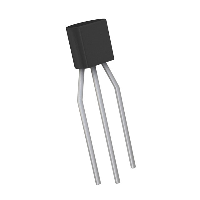
SOT-223
Notes: MSL 3 (Moisture Sensitivity Level) per J-STD-020
ABSOLUTE MAXIMUM RATINGS (TA = 25°C unless otherwise noted)
PARAMETER
SYMBOL
LIMIT
UNIT
Collector-Base Voltage
VCBO
600
V
Collector-Emitter Voltage
VCES
600
V
Collector-Emitter Voltage @ VBE=0V
VCES
400
V
Emitter-Base Voltage
VEBO
7
V
0.3
A
1
A
DC
Collector Current
IC
Pulse
Power Total Dissipation @ TA=25ºC
PDTOT
Maximum Operating Junction Temperature
W
+150
o
TSTG
-55 to +150
o
SYMBOL
LIMIT
RӨJA
91
o
25
o
TJ
Storage Temperature Range
1
C
C
THERMAL PERFORMANCE
PARAMETER
Junction to Ambient Thermal Resistance
Junction to Case Thermal Resistance
RӨJC
1
UNIT
C/W
C/W
Version: F1801
�TSC966CW
Taiwan Semiconductor
ELECTRICAL SPECIFICATIONS (TA = 25°C unless otherwise noted)
PARAMETER
Static
CONDITIONS
SYMBOL
MIN
TYP
MAX
UNIT
(Note 1)
Collector-Base voltage
IC =50μA
BVCBO
600
--
--
V
Collector-Emitter Saturation Voltage
IC =100μA, VBE =0
BVCES
600
--
--
V
Collector-Emitter breakdown voltage
IC =1mA
BVCEO
400
--
--
V
Emitter-Base breakdown voltage
IE =50μA
BVEBO
7
--
--
V
Emitter cut-off current
VEB =7V
IEBO
--
--
1.5
µA
Collector cut-off current
VCB =600V
ICBO
--
--
0.5
µA
Collector-Emitter Cutoff Current
VCE =400V
ICEO
--
--
1
µA
Collector-Emitter saturation voltage
IC =50mA, IB =5mA
VCE(SAT)
---
--
0.5
V
Base-Emitter saturation voltage
IC =50mA, IB =5mA
VBE(SAT)
--
--
1
V
VCE =5V, IC =1mA
hFE1
100
--
--
VCE =5V, IC =20mA
hFE2
90
--
300
DC Current Gain
Transition Frequency
VCE = 10V, IE =20mA
fT
50
--
--
MHz
Output Capacitance
VCB =20V, f =1MHz
Cob
--
--
7
pF
Notes:
1.
Pulse test: ≤ 380µs, duty cycle ≤ 2%
2.
For DESIGN AID ONLY, not subject to production testing.
ORDERING INFORMATION
PART NO.
PACKAGE
PACKING
TSC966CW RPG
SOT-223
2,500pcs / 13”Reel
2
Version: F1801
�TSC966CW
Taiwan Semiconductor
Electrical Characteristics Curve
(Ta = 25oC, unless otherwise noted)
Figure 1. Static Characteristics
Figure 2. DC Current Gain
Figure 3. DC Current Gain
Figure 4. VCE(sat) vs Ic
Figure 5. VBE(sat) vs Ic
Figure 6. Safety Operation Area
3
Version: F1801
�TSC966CW
Taiwan Semiconductor
PACKAGE OUTLINE DIMENSIONS (Unit: Millimeters)
SOT-223
SUGGESTED PAD LAYOUT (Unit: Millimeters)
Marking Diagram
Y
M
L
= Year Code
= Month Code for Halogen Free Product
O =Jan P =Feb Q =Mar R =Apr
S =May T =Jun U =Jul
V =Aug
W =Sep X =Oct
Y =Nov Z =Dec
= Lot Code
4
Version: F1801
�TSC966CW
Taiwan Semiconductor
Notice
Specifications of the products displayed herein are subject to change without notice. TSC or anyone on its behalf,
assumes no responsibility or liability for any errors or inaccuracies.
Information contained herein is intended to provide a product description only. No license, express or implied, to
any intellectual property rights is granted by this document. Except as provided in TSC’s terms and conditions of
sale for such products, TSC assumes no liability whatsoever, and disclaims any express or implied warranty,
relating to sale and/or use of TSC products including liability or warranties relating to fitness for a particular purpose,
merchantability, or infringement of any patent, copyright, or other intellectual property right.
The products shown herein are not designed for use in medical, life-saving, or life-sustaining applications.
Customers using or selling these products for use in such applications do so at their own risk and agree to fully
indemnify TSC for any damages resulting from such improper use or sale.
5
Version: F1801
�
很抱歉,暂时无法提供与“TSC966CT A3G”相匹配的价格&库存,您可以联系我们找货
免费人工找货