TSM301K12
20V P-Channel MOSFET with Schottky Diode
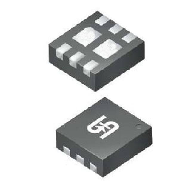
TDFN 2x2
PRODUCT SUMMARY
VDS (V)
RDS(on)(mΩ)
Pin Definition:
1. Anode
6. Cathode
2. NC
5. Gate
3. Drain
4. Source
-20
ID (A)
94 @ VGS = -4.5V
-2.8
131 @ VGS = -2.5V
-2.3
185 @ VGS = -1.8V
-0.54
SCHOTTKY PRODUCT SUMMARY
VR (V)
VF (V)
IF (A)
20
0.5
2
Block Diagram
Features
●
Configuration with MOSFET and Low Vf SKY
●
Package low profile 0.75mm (Typ)
●
Independent Pin Out for Design Flexibility
Application
●
Load Switch for Portable Applications
●
DC-DC Buck Circuit
●
Li-ion Battery Applications
●
Cellular Charger Switch
Ordering Information
Part No.
Package
TSM301K12CQ RFG
TDFN 2x2
Note: “G” denotes for Halogen Free
P-Channel MOSFET with Schottky Diode
Packing
3Kpcs / 7” Reel
MOSFET Absolute Maximum Rating (TA=25oC unless otherwise noted)
Parameter
Symbol
Limit
Unit
Drain-Source Voltage
VDS
-20
V
Gate-Source Voltage
VGS
±12
V
ID
-4.5
A
IDM
-8
A
6.5
W
Continuous Drain Current (Note 1,2)
Pulsed Drain Current
o
Maximum Power Dissipation
TC=25 C
o
TA=25 C (Note 2)
Operating Junction Temperature
PD
TJ
Operating Junction and Storage Temperature Range
TJ, TSTG
1.56
W
+150
o
- 55 to +150
o
C
C
Schottky Absolute Maximum Rating (TA=25oC unless otherwise noted)
Parameter
Symbol
Limit
Unit
Reverse Voltage
VR
20
V
Average Forward Current (Note 1,2)
IF
2
A
IFM
5
A
6.8
W
1.47
W
Pulsed Forward Current
o
Maximum Power Dissipation (Note 1)
TC=25 C
o
TA=25 C (Note 2)
1/7
PD
Version: C12
�TSM301K12
20V P-Channel MOSFET with Schottky Diode
Thermal Resistance Ratings
Parameter
Symbol
Limit
Unit
T≤ 5s
Steady State
80
120
o
RӨJA
T ≤ 5s
Steady State
85
130
o
RӨJA
MOSFET
Thermal Resistance-Junction to Ambient
C/W
C/W
o
Schottky
Thermal Resistance-Junction to Ambient
C/W
C/W
o
Notes:
1. Surface mounted on 1” x 1” (2 oz) FAR4 board,
2. t ≤ 5s
MOSFET Electrical Specifications (Ta = 25oC unless otherwise noted)
Parameter
Conditions
Symbol
Min
Typ
Max
Unit
Static
Drain-Source Breakdown Voltage
VGS = 0V, ID = -250uA
BVDSS
-20
--
--
V
Gate Threshold Voltage
VDS = VGS, ID = -250µA
VGS(TH)
-0.5
--
--
V
Gate Body Leakage
VGS = ±12V, VDS = 0V
IGSS
--
--
±100
nA
Zero Gate Voltage Drain Current
VDS =-20V, VGS = 0V
IDSS
--
--
-1
µA
--
--
94
--
--
131
--
--
185
VSD
--
--
-1.2
Qg
--
5.2
10
Qgs
--
1.36
--
Qgd
--
0.6
--
Ciss
--
5.2
--
Coss
--
9.7
--
Crss
--
19
--
td(on)
--
29
--
tr
--
295
--
td(off)
--
170
--
tf
--
65
--
Symbol
Min
Typ
Max
Unit
VF
--
--
0.5
V
--
0.015
0.08
--
0.02
0.10
--
60
--
VGS = -4.5V, ID = -2.8A
a
Drain-Source On-State Resistance
VGS = -2.5V, ID = -2.3A
RDS(ON)
VGS = -1.8V, ID = -0.54A
Diode Forward Voltage
IS = -1.6A, VGS = 0V
mΩ
V
b
Dynamic
Total Gate Charge
Gate-Source Charge
Gate-Drain Charge
Input Capacitance
Output Capacitance
Reverse Transfer Capacitance
Switching
VDS = -6V, ID = -2.8A,
VGS = -5V
VGS=0V, VDS=-6V,
f =1.0MHz
nC
pF
c
Turn-On Delay Time
Turn-On Rise Time
VDS=-15V, RD=15Ω,
Turn-Off Delay Time
RG=6Ω, VGS=-10V
Turn-Off Fall Time
nS
Schottky Electrical Specifications (Ta = 25oC unless otherwise noted)
Parameter
Conditions
Forward Voltage Drop
IF = 1A
Maximum Reverse Leakage
VR = 5V
Current
VR = 20V
IRm
Junction Capacitance
VR = 10V
CT
Notes:
a. pulse test: PW ≤300µS, duty cycle ≤2%
b. For DESIGN AID ONLY, not subject to production testing.
c. Switching time is essentially independent of operating temperature.
2/7
mA
pF
Version: C12
�TSM301K12
20V P-Channel MOSFET with Schottky Diode
MOSFET Electrical Characteristics Curve (Ta = 25oC, unless otherwise noted)
Output Characteristics
Transfer Characteristics
On-Resistance vs. Drain Current
Gate Charge
On-Resistance vs. Junction Temperature
Source-Drain Diode Forward Voltage
3/7
Version: C12
�TSM301K12
20V P-Channel MOSFET with Schottky Diode
Electrical Characteristics Curve (Ta = 25oC, unless otherwise noted)
On-Resistance vs. Gate-Source Voltage
Threshold Voltage
Single Pulse Power
Normalized Thermal Transient Impedance, Junction-to-Ambient
4/7
Version: C12
�TSM301K12
20V P-Channel MOSFET with Schottky Diode
SCHOTTKY Electrical Characteristics Curve (Ta = 25oC, unless otherwise noted)
Typical Forward Current Derating Curve
Typical Instantaneous Forward Characteristics
Typical Reverse Characteristics
Typical Junction Capacitance
Maximum Repetitive Forward Surge Current
5/7
Version: C12
�TSM301K12
20V P-Channel MOSFET with Schottky Diode
TDFN 2x2 Mechanical Drawing
DIM
A
B
C
D
E
F
G
H
J
K
MILLIMETERS
MIN
MAX
1.95
2.05
1.95
2.05
0.50
0.60
0.30
0.40
0.20
0.30
0.65 BSC
0.75
0.85
0.70
0.80
-0.05
0.195
0.211
INCHES
MIN
MAX
0.0768
0.0807
0.0768
0.0807
0.0197
0.0236
0.0118
0.0157
0.0079
0.0118
0.0256 BSC
0.0295
0.0335
0.0276
0.0315
0.0020
0.0077
0.0083
Marking Diagram
Y = Year Code
M = Month Code for Halogen Free Product
(O=Jan, P=Feb, Q=Mar, R=Apl, S=May, T=Jun, U=Jul, V=Aug, W=Sep,
X=Oct, Y=Nov, Z=Dec)
L = Lot Code
6/7
Version: C12
�TSM301K12
20V P-Channel MOSFET with Schottky Diode
Notice
Specifications of the products displayed herein are subject to change without notice. TSC or anyone on its behalf,
assumes no responsibility or liability for any errors or inaccuracies.
Information contained herein is intended to provide a product description only. No license, express or implied, to
any intellectual property rights is granted by this document. Except as provided in TSC’s terms and conditions of
sale for such products, TSC assumes no liability whatsoever, and disclaims any express or implied warranty,
relating to sale and/or use of TSC products including liability or warranties relating to fitness for a particular purpose,
merchantability, or infringement of any patent, copyright, or other intellectual property right.
The products shown herein are not designed for use in medical, life-saving, or life-sustaining applications.
Customers using or selling these products for use in such applications do so at their own risk and agree to fully
indemnify TSC for any damages resulting from such improper use or sale.
7/7
Version: C12
�


 工商网监
湘ICP备2023018690号
工商网监
湘ICP备2023018690号