HUF75343G3, HUF75343P3, HUF75343S3,
HUF75343S3S
Data Sheet
75A, 55V, 0.009 Ohm, N-Channel UltraFET
Power MOSFETs
These N-Channel power MOSFETs
are manufactured using the
innovative UltraFET® process. This
advanced process technology
achieves the lowest possible onresistance per silicon area, resulting in outstanding
performance. This device is capable of withstanding high
energy in the avalanche mode and the diode exhibits very
low reverse recovery time and stored charge. It was
designed for use in applications where power efficiency is
important, such as switching regulators, switching
converters, motor drivers, relay drivers, low-voltage bus
switches, and power management in portable and battery
operated products.
March 2003
Features
• 75A, 55V
• Simulation Models
- Temperature Compensating PSPICE® and SABER™
Models
- Thermal Impedance PSPICE™ and SABER Models
Available on the WEB at: www.fairchildsemi.com
• Peak Current vs Pulse Width Curve
• UIS Rating Curve
• Related Literature
- TB334, “Guidelines for Soldering Surface Mount
Components to PC Boards”
Symbol
Formerly developmental type TA75343.
Ordering Information
PART NUMBER
D
PACKAGE
BRAND
HUF75343G3
TO-247
75343G
HUF75343P3
TO-220AB
75343P
HUF75343S3
TO-262AA
75343S
HUF75343S3S
TO-263AB
75343S
G
S
NOTE: When ordering, use the entire part number. Add the suffix T to
obtain the TO-263AB variant in tape and reel, e.g., HUF75343S3ST.
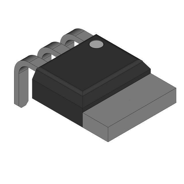
Packaging
JEDEC STYLE TO-247
JEDEC TO-220AB
SOURCE
DRAIN
GATE
SOURCE
DRAIN
GATE
DRAIN
(FLANGE)
DRAIN
(TAB)
JEDEC TO-263AB
JEDEC TO-262AA
SOURCE
DRAIN
GATE
GATE
SOURCE
DRAIN
(FLANGE)
DRAIN
(FLANGE)
Product reliability information can be found at http://www.fairchildsemi.com/products/discrete/reliability/index.html
For severe environments, see our Automotive HUFA series.
All Fairchild semiconductor products are manufactured, assembled and tested under ISO9000 and QS9000 quality systems certification.
©2003 Fairchild Semiconductor Corporation
HUF75343G3, HUF75343P3, HUF75343S3, HUF75343S3S Rev. B1
�HUF75343G3, HUF75343P3, HUF75343S3, HUF75343S3S
Absolute Maximum Ratings
TC = 25oC, Unless Otherwise Specified
UNITS
V
V
V
55
55
±20
Drain to Source Voltage (Note 1) . . . . . . . . . . . . . . . . . . . . . . . VDSS
Drain to Gate Voltage (RGS = 20kΩ) (Note 1) . . . . . . . . . . . . . VDGR
Gate to Source Voltage . . . . . . . . . . . . . . . . . . . . . . . . . . . . . . . VGS
Drain Current
Continuous (Figure 2). . . . . . . . . . . . . . . . . . . . . . . . . . . . . . . . . ID
Pulsed Drain Current . . . . . . . . . . . . . . . . . . . . . . . . . . . . . . . . IDM
Pulsed Avalanche Rating . . . . . . . . . . . . . . . . . . . . . . . . . . . . . . EAS
Power Dissipation . . . . . . . . . . . . . . . . . . . . . . . . . . . . . . . . . . . . PD
Derate Above 25oC . . . . . . . . . . . . . . . . . . . . . . . . . . . . . . . . . . . .
Operating and Storage Temperature . . . . . . . . . . . . . . . . . .TJ, TSTG
Maximum Temperature for Soldering
Leads at 0.063in (1.6mm) from Case for 10s. . . . . . . . . . . . . . . TL
Package Body for 10s, See Techbrief 334 . . . . . . . . . . . . . . . Tpkg
75
Figure 4
Figure 6
270
1.81
-55 to 175
A
W
W/oC
oC
300
260
oC
oC
CAUTION: Stresses above those listed in “Absolute Maximum Ratings” may cause permanent damage to the device. This is a stress only rating and operation of the
device at these or any other conditions above those indicated in the operational sections of this specification is not implied.
NOTE:
1. TJ = 25oC to 150oC.
Electrical Specifications
TC = 25oC, Unless Otherwise Specified
PARAMETER
SYMBOL
TEST CONDITIONS
MIN
TYP
MAX
UNITS
55
-
-
V
VDS = 50V, VGS = 0V
-
-
1
µA
VDS = 45V, VGS = 0V, TC = 150oC
-
-
250
µA
VGS = ±20V
-
-
±100
nA
OFF STATE SPECIFICATIONS
Drain to Source Breakdown Voltage
Zero Gate Voltage Drain Current
Gate to Source Leakage Current
BVDSS
IDSS
IGSS
ID = 250µA, VGS = 0V (Figure 11)
ON STATE SPECIFICATIONS
Gate to Source Threshold Voltage
VGS(TH)
VGS = VDS, ID = 250µA (Figure 10)
2
-
4
V
Drain to Source On Resistance
rDS(ON)
ID = 75A, VGS = 10V (Figure 9)
-
0.007
0.009
Ω
THERMAL SPECIFICATIONS
Thermal Resistance Junction to Case
RθJC
(Figure 3)
-
-
0.55
oC/W
Thermal Resistance Junction to Ambient
RθJA
TO-247
-
-
30
oC/W
TO-220, TO-263
-
-
62
oC/W
VDD = 30V, ID ≅ 75A,
RL = 0.4Ω, VGS = 10V,
RGS = 2.5Ω
-
-
125
ns
-
9
-
ns
tr
-
75
-
ns
td(OFF)
-
32
-
ns
tf
-
18
-
ns
tOFF
-
-
75
ns
-
170
205
nC
-
92
110
nC
-
6.0
7.2
nC
-
13
-
nC
-
42
-
nC
SWITCHING SPECIFICATIONS (VGS = 10V)
Turn-On Time
Turn-On Delay Time
Rise Time
Turn-Off Delay Time
Fall Time
Turn-Off Time
tON
td(ON)
GATE CHARGE SPECIFICATIONS
Qg(TOT)
VGS = 0V to 20V
Gate Charge at 10V
Qg(10)
VGS = 0V to 10V
Threshold Gate Charge
Qg(TH)
VGS = 0V to 2V
Total Gate Charge
Gate to Source Gate Charge
Qgs
Gate to Drain “Miller” Charge
Qgd
©2003 Fairchild Semiconductor Corporation
VDD = 30V,
ID ≅ 75A,
RL = 0.4Ω
Ig(REF) = 1.0mA
(Figure 13)
HUF75343G3, HUF75343P3, HUF75343S3, HUF75343S3S Rev. B1
�HUF75343G3, HUF75343P3, HUF75343S3, HUF75343S3S
TC = 25oC, Unless Otherwise Specified
Electrical Specifications
PARAMETER
SYMBOL
TEST CONDITIONS
MIN
TYP
MAX
UNITS
-
3000
-
pF
-
1100
-
pF
-
230
-
pF
CAPACITANCE SPECIFICATIONS
Input Capacitance
CISS
Output Capacitance
COSS
Reverse Transfer Capacitance
CRSS
VDS = 25V, VGS = 0V,
f = 1MHz
(Figure 12)
Source to Drain Diode Specifications
PARAMETER
SYMBOL
Source to Drain Diode Voltage
TEST CONDITIONS
MIN
TYP
MAX
UNITS
ISD = 75A
-
-
1.25
V
trr
ISD = 75A, dISD/dt = 100A/µs
-
-
100
ns
QRR
ISD = 75A, dISD/dt = 100A/µs
-
-
200
nC
VSD
Reverse Recovery Time
Reverse Recovered Charge
Typical Performance Curves
80
1.0
ID, DRAIN CURRENT (A)
POWER DISSIPATION MULTIPLIER
1.2
0.8
0.6
0.4
60
40
20
0.2
0
0
0
25
50
75
100
125
150
25
175
50
TC , CASE TEMPERATURE (oC)
75
100
125
150
175
TC, CASE TEMPERATURE (oC)
FIGURE 1. NORMALIZED POWER DISSIPATION vs CASE
TEMPERATURE
FIGURE 2. MAXIMUM CONTINUOUS DRAIN CURRENT vs
CASE TEMPERATURE
2
ZθJC, NORMALIZED
THERMAL IMPEDANCE
1
DUTY CYCLE - DESCENDING ORDER
0.5
0.2
0.1
0.05
0.02
0.01
PDM
0.1
t1
t2
NOTES:
DUTY FACTOR: D = t1/t2
PEAK TJ = PDM x ZθJC x RθJC + TC
SINGLE PULSE
0.01
10-5
10-4
10-3
10-2
10-1
100
101
t, RECTANGULAR PULSE DURATION (s)
FIGURE 3. NORMALIZED MAXIMUM TRANSIENT THERMAL IMPEDANCE
©2003 Fairchild Semiconductor Corporation
HUF75343G3, HUF75343P3, HUF75343S3, HUF75343S3S Rev. B1
�HUF75343G3, HUF75343P3, HUF75343S3, HUF75343S3S
Typical Performance Curves
(Continued)
2000
TC = 25oC
IDM, PEAK CURRENT (A)
1000
FOR TEMPERATURES
ABOVE 25oC DERATE PEAK
CURRENT AS FOLLOWS:
175 - TC
I = I25
150
VGS = 10V
100
TRANSCONDUCTANCE
MAY LIMIT CURRENT
IN THIS REGION
50
10-5
10-4
10-3
10-2
10-1
100
101
t, PULSE WIDTH (s)
FIGURE 4. PEAK CURRENT CAPABILITY
500
TJ = MAX RATED
TC = 25oC
100
100
100µs
1ms
10
OPERATION IN THIS
AREA MAY BE
LIMITED BY rDS(ON)
VDSS(MAX) = 55V
If R = 0
tAV = (L)(IAS)/(1.3*RATED BVDSS - VDD)
If R ≠ 0
tAV = (L/R)ln[(IAS*R)/(1.3*RATED BVDSS - VDD) +1]
IAS, AVALANCHE CURRENT (A)
ID, DRAIN CURRENT (A)
1000
10ms
STARTING TJ = 25oC
STARTING TJ = 150oC
10
0.01
1
1
10
100
200
0.1
1
tAV, TIME IN AVALANCHE (ms)
10
VDS, DRAIN TO SOURCE VOLTAGE (V)
NOTE: Refer to Fairchild Application Notes AN9321 and AN9322.
FIGURE 5. FORWARD BIAS SAFE OPERATING AREA
FIGURE 6. UNCLAMPED INDUCTIVE SWITCHING CAPABILITY
150
VGS = 20V
VGS = 10V
VGS = 7V
ID, DRAIN CURRENT (A)
ID, DRAIN CURRENT (A)
150
100
VGS = 6V
50
VGS = 5V
VDD = 15V
PULSE DURATION = 80µs
DUTY CYCLE = 0.5% MAX
0
0.5
1.0
1.5
2.0
2.5
3.0
3.5
VDS, DRAIN TO SOURCE VOLTAGE (V)
FIGURE 7. SATURATION CHARACTERISTICS
©2003 Fairchild Semiconductor Corporation
4.0
175oC
100
50
PULSE DURATION = 80µs
DUTY CYCLE = 0.5% MAX
TC = 25oC
0
-55oC
25oC
0
0
1.5
3.0
4.5
6.0
VGS, GATE TO SOURCE VOLTAGE (V)
7.5
FIGURE 8. TRANSFER CHARACTERISTICS
HUF75343G3, HUF75343P3, HUF75343S3, HUF75343S3S Rev. B1
�HUF75343G3, HUF75343P3, HUF75343S3, HUF75343S3S
Typical Performance Curves
(Continued)
1.2
PULSE DURATION = 80µs
DUTY CYCLE = 0.5% MAX
VGS = 10V, ID = 75A
VGS = VDS, ID = 250µA
NORMALIZED GATE
THRESHOLD VOLTAGE
NORMALIZED DRAIN TO SOURCE
ON RESISTANCE
2.5
2.0
1.5
1.0
0.5
1.0
0.8
0.6
-80
-40
0
40
80
120
160
-80
200
-40
TJ, JUNCTION TEMPERATURE (oC)
40
80
120
160
200
TJ, JUNCTION TEMPERATURE (oC)
FIGURE 9. NORMALIZED DRAIN TO SOURCE ON
RESISTANCE vs JUNCTION TEMPERATURE
FIGURE 10. NORMALIZED GATE THRESHOLD VOLTAGE vs
JUNCTION TEMPERATURE
4000
1.2
VGS = 0V, f = 1MHz
CISS = CGS + CGD
CRSS = CGD
COSS ≈ CDS + CGD
ID = 250µA
C, CAPACITANCE (pF)
NORMALIZED DRAIN TO SOURCE
BREAKDOWN VOLTAGE
0
1.1
1.0
3000
CISS
2000
COSS
1000
CRSS
0.9
-80
-40
0
40
80
120
160
200
0
0
10
TJ , JUNCTION TEMPERATURE (oC)
20
30
40
50
60
VDS , DRAIN TO SOURCE VOLTAGE (V)
FIGURE 11. NORMALIZED DRAIN TO SOURCE BREAKDOWN
VOLTAGE vs JUNCTION TEMPERATURE
FIGURE 12. CAPACITANCE vs DRAIN TO SOURCE VOLTAGE
VGS , GATE TO SOURCE VOLTAGE (V)
10
8
6
4
2
VDD = 30V
0
0
20
WAVEFORMS IN
DESCENDING ORDER:
ID = 75A
ID = 47A
ID = 18A
60
40
Qg, GATE CHARGE (nC)
80
100
NOTE: Refer to Fairchild Application Notes AN7254 and AN7260.
FIGURE 13. GATE CHARGE WAVEFORMS FOR CONSTANT GATE CURRENT
©2003 Fairchild Semiconductor Corporation
HUF75343G3, HUF75343P3, HUF75343S3, HUF75343S3S Rev. B1
�HUF75343G3, HUF75343P3, HUF75343S3, HUF75343S3S
Test Circuits and Waveforms
VDS
BVDSS
L
tP
VARY tP TO OBTAIN
REQUIRED PEAK IAS
IAS
+
RG
VDS
VDD
VDD
-
VGS
DUT
tP
0V
IAS
0
0.01Ω
tAV
FIGURE 14. UNCLAMPED ENERGY TEST CIRCUIT
FIGURE 15. UNCLAMPED ENERGY WAVEFORMS
VDS
VDD
RL
Qg(TOT)
VDS
VGS = 20V
VGS
Qg(10)
+
VDD
VGS = 10V
VGS
DUT
VGS = 2V
IG(REF)
0
Qg(TH)
Qgs
Qgd
Ig(REF)
0
FIGURE 16. GATE CHARGE TEST CIRCUIT
FIGURE 17. GATE CHARGE WAVEFORM
VDS
tON
tOFF
td(ON)
td(OFF)
tr
RL
VDS
tf
90%
90%
+
VGS
-
VDD
10%
0
10%
DUT
90%
RGS
VGS
VGS
0
FIGURE 18. SWITCHING TIME TEST CIRCUIT
©2003 Fairchild Semiconductor Corporation
10%
50%
50%
PULSE WIDTH
FIGURE 19. RESISTIVE SWITCHING WAVEFORMS
HUF75343G3, HUF75343P3, HUF75343S3, HUF75343S3S Rev. B1
�HUF75343G3, HUF75343P3, HUF75343S3, HUF75343S3S
PSPICE Electrical Model
.SUBCKT HUF75343 2 1 3 ;
rev 9Feb99
CA 12 8 3.95e-9
CB 15 14 5.05e-9
CIN 6 8 2.68e-9
LDRAIN
DPLCAP
DRAIN
2
5
10
DBODY 7 5 DBODYMOD
DBREAK 5 11 DBREAKMOD
DPLCAP 10 5 DPLCAPMOD
DBREAK
+
RSLC2
5
51
ESLC
11
-
EBREAK 11 7 17 18 58.39
EDS 14 8 5 8 1
EGS 13 8 6 8 1
ESG 6 10 6 8 1
EVTHRES 6 21 19 8 1
EVTEMP 20 6 18 22 1
IT 8 17 1
RLDRAIN
RSLC1
51
RDRAIN
6
8
ESG
EVTHRES
+ 19 8
+
LGATE
EVTEMP
RGATE +
18 22
9
20
GATE
1
LDRAIN 2 5 1e-9
LGATE 1 9 2.60e-9
LSOURCE 3 7 1.1e-9
KGATE LSOURCE LGATE 0.0085
+
50
-
21
EBREAK
17
18
DBODY
-
16
MWEAK
6
MMED
MSTRO
RLGATE
LSOURCE
CIN
8
SOURCE
3
7
RSOURCE
RLSOURCE
MMED 16 6 8 8 MMEDMOD
MSTRO 16 6 8 8 MSTROMOD
MWEAK 16 21 8 8 MWEAKMOD
S1A
12
RBREAK 17 18 RBREAKMOD 1
RDRAIN 50 16 RDRAINMOD 0.70e-3
RGATE 9 20 0.36
RLDRAIN 2 5 10
RLGATE 1 9 26
RLSOURCE 3 7 11
RSLC1 5 51 RSLCMOD 1e-6
RSLC2 5 50 1e3
RSOURCE 8 7 RSOURCEMOD 4.79e-3
RVTHRES 22 8 RVTHRESMOD 1
RVTEMP 18 19 RVTEMPMOD 1
S1A
S1B
S2A
S2B
S2A
14
13
13
8
S1B
CA
RBREAK
15
17
18
RVTEMP
S2B
13
CB
6
8
EGS
19
-
-
IT
14
+
+
VBAT
5
8
EDS
-
+
8
22
RVTHRES
6 12 13 8 S1AMOD
13 12 13 8 S1BMOD
6 15 14 13 S2AMOD
13 15 14 13 S2BMOD
VBAT 22 19 DC 1
ESLC 51 50 VALUE={(V(5,51)/ABS(V(5,51)))*(PWR(V(5,51)/(1e-6*609),2.5))}
.MODEL DBODYMOD D (IS = 2.35e-12 RS = 2.21e-3 TRS1 = 2.47e-3 TRS2 = 3.97e-11 CJO = 6.34e-9 TT = 3.95e-8 M = 0.6)
.MODEL DBREAKMOD D (RS = 9.1e-2 TRS1 = -2.24e-4 TRS2 = 5.23e-6)
.MODEL DPLCAPMOD D (CJO = 2.15e-9 IS = 1e-30 N = 10 M= 0.73)
.MODEL MMEDMOD NMOS (VTO = 3.30 KP = 5.49 IS = 1e-30 N = 10 TOX = 1 L = 1u W = 1u RG = 0.36)
.MODEL MSTROMOD NMOS (VTO = 3.87 KP = 145 IS = 1e-30 N = 10 TOX = 1 L = 1u W = 1u)
.MODEL MWEAKMOD NMOS (VTO = 2.92 KP = 0.05 IS = 1e-30 N = 10 TOX = 1 L = 1u W = 1u RG = 3.6 RS =.1)
.MODEL RBREAKMOD RES (TC1 = 1.04e-3 TC2 = 3.43e-7)
.MODEL RDRAINMOD RES (TC1 = 4.44e-2 TC2 = 8.04e-5)
.MODEL RSLCMOD RES (TC1 = 1.02e-4 TC2 = 2.07e-6)
.MODEL RSOURCEMOD RES (TC1 = 0 TC2 = 0)
.MODEL RVTHRESMOD RES (TC1 = -3.49e-3 TC2 = -1.27e-5)
.MODEL RVTEMPMOD RES (TC1 = -1.93e-3 TC2 = 1.38e-6)
.MODEL S1AMOD VSWITCH (RON = 1e-5
.MODEL S1BMOD VSWITCH (RON = 1e-5
.MODEL S2AMOD VSWITCH (RON = 1e-5
.MODEL S2BMOD VSWITCH (RON = 1e-5
ROFF = 0.1
ROFF = 0.1
ROFF = 0.1
ROFF = 0.1
VON = -6.90 VOFF= -3.90)
VON = -3.90 VOFF= -6.90)
VON = 0.39 VOFF= 3.39)
VON = 3.39 VOFF= 0.39)
.ENDS
NOTE: For further discussion of the PSPICE model, consult A New PSPICE Sub-Circuit for the Power MOSFET Featuring Global
Temperature Options; IEEE Power Electronics Specialist Conference Records, 1991, written by William J. Hepp and C. Frank Wheatley.
©2003 Fairchild Semiconductor Corporation
HUF75343G3, HUF75343P3, HUF75343S3, HUF75343S3S Rev. B1
�HUF75343G3, HUF75343P3, HUF75343S3, HUF75343S3S
SABER Electrical Model
REV February 1999
template huf75343 n2, n1, n3
electrical n2, n1, n3
{
var i iscl
d..model dbodymod = (is = 2.35e-12, cjo = 6.34e-9, tt = 3.950e-8, m = 0.6)
d..model dbreakmod = ()
d..model dplcapmod = (cjo = 21.5e-10, is = 1e-30, n = 10, m = 0.730)
m..model mmedmod = (type=_n, vto = 3.30, kp = 5.49, is = 1e-30, tox = 1)
m..model mstrongmod = (type=_n, vto = 3.87, kp = 145, is = 1e-30, tox = 1)
m..model mweakmod = (type=_n, vto = 2.92, kp = 0.050, is = 1e-30, tox = 1)
sw_vcsp..model s1amod = (ron = 1e-5, roff = 0.1, von = -6.90, voff = -3.90)
sw_vcsp..model s1bmod = (ron = 1e-5, roff = 0.1, von = -3.90, voff = -6.90)
sw_vcsp..model s2amod = (ron = 1e-5, roff = 0.1, von = 0.39, voff = 3.39)
sw_vcsp..model s2bmod = (ron = 1e-5, roff = 0.1, von = 3.39, voff = 0.39)
10
RSLC1
51
i.it n8 n17 = 1
RDRAIN
6
8
EVTHRES
+ 19 8
21
DBODY
EBREAK
+
17
18
MSTRO
-
8
LSOURCE
7
SOURCE
3
RSOURCE
RLSOURCE
S1A
12
m.mmed n16 n6 n8 n8 = model=mmedmod, l = 1u, w = 1u
m.mstrong n16 n6 n8 n8 = model=mstrongmod, l = 1u, w = 1u
m.mweak n16 n21 n8 n8 = model=mweakmod, l = 1u, w = 1u
res.rbreak n17 n18 = 1, tc1 = 1.04e-3, tc2 = 3.43e-7
res.rdbody n71 n5 = 2.21e-3, tc1 = 2.47e-3, tc2 = 3.97e-11
res.rdbreak n72 n5 = 9.1e-2, tc1 = -2.24e-4, tc2 = 5.23e-6
res.rdrain n50 n16 = 0.70e-3, tc1 = 4.44e-2, tc2 = 8.04e-5
res.rgate n9 n20 = 0.36
res.rldrain n2 n5 = 10
res.rlgate n1 n9 = 26.0
res.rlsource n3 n7 = 11.0
res.rslc1 n5 n51 = 1e-6, tc1 = 1.02e-4, tc2 = 2.07e-6
res.rslc2 n5 n50 = 1e3
res.rsource n8 n7 = 4.79e-3, tc1 = 0, tc2 = 0
res.rvtemp n18 n19 = 1, tc1 = -1.93e-3, tc2 = 1.38e-6
res.rvthres n22 n8 = 1, tc1 = -3.49e-3, tc2 = -1.27e-5
MWEAK
MMED
CIN
71
11
16
6
RLGATE
RDBODY
DBREAK
50
EVTEMP
RGATE + 18 22
9
20
l.ldrain n2 n5 = 1e-9
l.lgate n1 n9 = 2.60e-9
l.lsource n3 n7 = 1.10e-9
k.k1 i(l.lgate) i(l.lsource) = l(l.lgate), l(l.lsource), 0.0085
72
ISCL
+
GATE
1
RLDRAIN
RDBREAK
RSLC2
ESG
LGATE
DRAIN
2
5
-
c.ca n12 n8 = 3.95e-9
c.cb n15 n14 = 5.05e-9
c.cin n6 n8 = 2.68e-9
d.dbody n7 n71 = model=dbodymod
d.dbreak n72 n11 = model=dbreakmod
d.dplcap n10 n5 = model=dplcapmod
LDRAIN
DPLCAP
S2A
14
13
13
8
S1B
CA
RBREAK
15
17
18
RVTEMP
S2B
13
CB
6
8
EGS
19
-
-
IT
14
+
+
VBAT
5
8
EDS
-
+
8
22
RVTHRES
spe.ebreak n11 n7 n17 n18 = 58.39
spe.eds n14 n8 n5 n8 = 1
spe.egs n13 n8 n6 n8 = 1
spe.esg n6 n10 n6 n8 = 1
spe.evtemp n20 n6 n18 n22 = 1
spe.evthres n6 n21 n19 n8 = 1
sw_vcsp.s1a n6 n12 n13 n8 = model=s1amod
sw_vcsp.s1b n13 n12 n13 n8 = model=s1bmod
sw_vcsp.s2a n6 n15 n14 n13 = model=s2amod
sw_vcsp.s2b n13 n15 n14 n13 = model=s2bmod
v.vbat n22 n19 = dc = 1
equations {
i (n51->n50) + = iscl
iscl: v(n51,n50) = ((v(n5,n51)/(1e-9+abs(v(n5,n51))))*((abs(v(n5,n51)*1e6/609))** 2.5))
}
}
©2003 Fairchild Semiconductor Corporation
HUF75343G3, HUF75343P3, HUF75343S3, HUF75343S3S Rev. B1
�HUF75343G3, HUF75343P3, HUF75343S3, HUF75343S3S
SPICE Thermal Model
th
JUNCTION
REV 12 February 1999
HUF75343
CTHERM1 th 6 6.15e-3
CTHERM2 6 5 2.50e-2
CTHERM3 5 4 1.40e-2
CTHERM4 4 3 1.25e-2
CTHERM5 3 2 4.85e-2
CTHERM6 2 tl 12.55
RTHERM1
RTHERM1 th 6 3.76e-3
RTHERM2 6 5 9.35e-3
RTHERM3 5 4 2.64e-2
RTHERM4 4 3 1.48e-1
RTHERM5 3 2 2.23e-1
RTHERM6 2 tl 2.96e-2
RTHERM2
CTHERM1
6
CTHERM2
5
CTHERM3
RTHERM3
SABER Thermal Model
SABER thermal model HUF75343
template thermal_model th tl
thermal_c th, tl
{
ctherm.ctherm1 th 6 = 6.15e-3
ctherm.ctherm2 6 5 = 2.50e-2
ctherm.ctherm3 5 4 = 1.40e-2
ctherm.ctherm4 4 3 = 1.25e-2
ctherm.ctherm5 3 2 = 4.85e-2
ctherm.ctherm6 2 tl = 12.55
rtherm.rtherm1 th 6 = 3.76e-3
rtherm.rtherm2 6 5 = 9.35e-3
rtherm.rtherm3 5 4 = 2.64e-2
rtherm.rtherm4 4 3 = 1.48e-1
rtherm.rtherm5 3 2 = 2.23e-1
rtherm.rtherm6 2 tl = 2.96e-2
}
4
CTHERM4
RTHERM4
3
CTHERM5
RTHERM5
2
CTHERM6
RTHERM6
tl
©2003 Fairchild Semiconductor Corporation
CASE
HUF75343G3, HUF75343P3, HUF75343S3, HUF75343S3S Rev. B1
�TRADEMARKS
The following are registered and unregistered trademarks Fairchild Semiconductor owns or is authorized to use and is not
intended to be an exhaustive list of all such trademarks.
ACEx™
FACT™
ActiveArray™
FACT Quiet Series™
Bottomless™
FAST®
CoolFET™
FASTr™
CROSSVOLT™ FRFET™
DOME™
GlobalOptoisolator™
EcoSPARK™
GTO™
E2CMOS™
HiSeC™
I2C™
EnSigna™
Across the board. Around the world.™
The Power Franchise™
Programmable Active Droop™
ImpliedDisconnect™
ISOPLANAR™
LittleFET™
MicroFET™
MicroPak™
MICROWIRE™
MSX™
MSXPro™
OCX™
OCXPro™
OPTOLOGIC®
OPTOPLANAR™
PACMAN™
POP™
Power247™
PowerTrench®
QFET™
QS™
QT Optoelectronics™
Quiet Series™
RapidConfigure™
RapidConnect™
SILENT SWITCHER®
SMART START™
SPM™
Stealth™
SuperSOT™-3
SuperSOT™-6
SuperSOT™-8
SyncFET™
TinyLogic®
TruTranslation™
UHC™
UltraFET®
VCX™
DISCLAIMER
FAIRCHILD SEMICONDUCTOR RESERVES THE RIGHT TO MAKE CHANGES WITHOUT FURTHER NOTICE TO ANY
PRODUCTS HEREIN TO IMPROVE RELIABILITY, FUNCTION OR DESIGN. FAIRCHILD DOES NOT ASSUME ANY
LIABILITY ARISING OUT OF THE APPLICATION OR USE OF ANY PRODUCT OR CIRCUIT DESCRIBED HEREIN;
NEITHER DOES IT CONVEY ANY LICENSE UNDER ITS PATENT RIGHTS, NOR THE RIGHTS OF OTHERS.
LIFE SUPPORT POLICY
FAIRCHILD’S PRODUCTS ARE NOT AUTHORIZED FOR USE AS CRITICAL COMPONENTS IN LIFE SUPPORT
DEVICES OR SYSTEMS WITHOUT THE EXPRESS WRITTEN APPROVAL OF FAIRCHILD SEMICONDUCTOR
CORPORATION.
As used herein:
1. Life support devices or systems are devices or systems
which, (a) are intended for surgical implant into the body,
or (b) support or sustain life, or (c) whose failure to perform
when properly used in accordance with instructions for use
provided in the labeling, can be reasonably expected to
result in significant injury to the user.
2. A critical component is any component of a life support
device or system whose failure to perform can be
reasonably expected to cause the failure of the life support
device or system, or to affect its safety or effectiveness.
PRODUCT STATUS DEFINITIONS
Definition of Terms
Datasheet Identification
Product Status
Definition
Advance Information
Formative or In
Design
This datasheet contains the design specifications for
product development. Specifications may change in
any manner without notice.
Preliminary
First Production
This datasheet contains preliminary data, and
supplementary data will be published at a later date.
Fairchild Semiconductor reserves the right to make
changes at any time without notice in order to improve
design.
No Identification Needed
Full Production
This datasheet contains final specifications. Fairchild
Semiconductor reserves the right to make changes at
any time without notice in order to improve design.
Obsolete
Not In Production
This datasheet contains specifications on a product
that has been discontinued by Fairchild semiconductor.
The datasheet is printed for reference information only.
Rev. I2
�