1N5221B - 1N5263B
Taiwan Semiconductor
500mW, 5% Tolerance Zener Diodes
FEATURES
KEY PARAMETERS
● Wide Zener voltage range selection: 2.4V to 56V
● VZ tolerance selection of ± 5%
● Compliant to RoHS directive 2011/65/EU and
in accordance to WEEE 2002/96/EC
● Halogen-free according to IEC 61249-2-21
PARAMETER
VALUE
UNIT
VZ
2.4-56
V
PD
500
mW
VF at IF=200mA
1.1
V
TJ Max.
200
°C
APPLICATIONS
●
●
●
●
Low voltage stabilizers or voltage references
Adapters
Lighting application
On-board DC/DC converter
Package
DO-35
Configuration
Single die
MECHANICAL DATA
● Case: DO-35
● Terminal: Matte tin plated leads, solderable per J-STD-002
● Polarity: Indicated by cathode band
ABSOLUTE MAXIMUM RATINGS (TA = 25°C unless otherwise noted)
PARAMETER
Power dissipation
SYMBOL
VALUE
UNIT
PD
500
mW
VF
1.1
V
Junction temperature range
TJ
200
°C
Storage temperature range
TSTG
200
°C
Forward voltage
IF=200mA
1
Version:G1804
�1N5221B - 1N5263B
Taiwan Semiconductor
ELECTRICAL SPECIFICATIONS (TA = 25°C unless otherwise noted)
ZENER VOLTAGE
TEST
TEST
LEAKAGE
CURRENT
CURRENT
ZZK @ IZK
IZK
IR @ V R
mA
REGULAR IMPEDANCE
CURRENT
PART NUMBER
VZ @ IZT
IZT
V
mA
Nominal
ZZT @ IZT
Ω
Ω
Max.
Max.
µA
V
Max.
1N5221B
2.4
20
30
1200
0.25
100
1.0
1N5222B
2.5
20
30
1250
0.25
100
1.0
1N5223B
2.7
20
30
1300
0.25
75
1.0
1N5224B
2.8
20
30
1400
0.25
75
1.0
1N5225B
3.0
20
29
1600
0.25
50.0
1.0
1N5226B
3.3
20
28
1600
0.25
25.0
1.0
1N5227B
3.6
20
24
1700
0.25
15.0
1.0
1N5228B
3.9
20
23
1900
0.25
10.0
1.0
1N5229B
4.3
20
22
2000
0.25
5.0
1.0
1N5230B
4.7
20
19
1900
0.25
5.0
2.0
1N5231B
5.1
20
17
1600
0.25
5.0
2.0
1N5232B
5.6
20
11
1600
0.25
5.0
3.0
1N5233B
6.0
20
7
1600
0.25
5.0
3.5
1N5234B
6.2
20
7
1000
0.25
5.0
4.0
1N5235B
6.8
20
5
750
0.25
3.0
5.0
1N5236B
7.5
20
6
500
0.25
3.0
6.0
1N5237B
8.2
20
8
500
0.25
3.0
6.5
1N5238B
8.7
20
8
600
0.25
3.0
6.5
1N5239B
9.1
20
10
600
0.25
3.0
7.0
1N5240B
10
20
17
600
0.25
2.0
8
1N5241B
11
20
22
600
0.25
1.0
8.4
1N5242B
12
20
30
600
0.25
0.5
9
1N5243B
13
9.5
13
600
0.25
0.1
10
1N5244B
14
9.0
15
600
0.25
0.1
10
1N5245B
15
8.5
16
600
0.25
0.1
11
1N5246B
16
7.8
17
600
0.25
0.1
12
1N5247B
17
7.4
19
600
0.25
0.1
13
1N5248B
18
7.0
21
600
0.25
0.1
14
1N5249B
19
6.6
23
600
0.25
0.1
14
1N5250B
20
6.2
25
600
0.25
0.1
15
1N5251B
22
5.6
29
600
0.25
0.1
17
1N5252B
24
5.2
33
600
0.25
0.1
18
1N5253B
25
5.0
35
600
0.25
0.1
18
1N5254B
27
4.6
41
600
0.25
0.1
21
1N5255B
28
4.5
44
600
0.25
0.1
21
1N5256B
30
4.2
49
600
0.25
0.1
23
1N5257B
33
3.8
58
700
0.25
0.1
25
1N5258B
36
3.4
70
700
0.25
0.1
27
2
Version:G1804
�1N5221B - 1N5263B
Taiwan Semiconductor
ELECTRICAL SPECIFICATIONS (TA = 25°C unless otherwise noted)
TEST
ZENER VOLTAGE
TEST
LEAKAGE
CURRENT
CURRENT
ZZK @ IZK
IZK
IR @ V R
mA
REGULAR IMPEDANCE
CURRENT
PART NUMBER
VZ @ IZT
IZT
V
mA
Nominal
ZZT @ IZT
Ω
Ω
Max.
Max.
µA
V
Max.
1N5259B
39
3.2
80
800
0.25
0.1
30
1N5260B
43
3.0
93
900
0.25
0.1
33
1N5261B
47
2.7
105
1000
0.25
0.1
36
1N5262B
51
2.5
125
1100
0.25
0.1
39
1N5263B
56
2.2
150
1300
0.25
0.1
43
Notes:
1. Nominal zener voltages between the voltages shown and tighter voltage, for detalied information on
price, availability and delivery.
2. The zener voltage(VZ) is tested under pulse condition. The measured VZ is guaranteed to be within
specification with device junction in thermal equilibrium.
3. Zener impedance is derived from the 60-cycle ac voltage, which results when an ac current having
an RMS value equal to 10% of the DC zener current (IZT) is superimposed to IZT.
4. Zener voltage has a standard tolerance on the nominal zener voltage of ±5%.
ORDERING INFORMATION
PART NO.
(Note 1)
PACKAGE
PACKING
1N52xxB R0
DO-35
10K / 14" Reel
1N52xxB R0G
DO-35
10K / 14" Reel
1N52xxB A0
DO-35
5K / Box (Ammo)
1N52xxB A0G
DO-35
5K / Box (Ammo)
Note:
1. "xx" defines part no. from 1N5221B to 1N5263B
3
Version:G1804
�1N5221B - 1N5263B
Taiwan Semiconductor
CHARACTERISTICS CURVES
(TA = 25°C unless otherwise noted)
Fig. 1 Power dissipation VS. Ambient temperature
600
PD - Power Dissipation (mW)
500
400
300
200
100
0
0
40
80
120
160
200
Tamb - Ambient Temperature (°C)
4
Version:G1804
�1N5221B - 1N5263B
Taiwan Semiconductor
PACKAGE OUTLINE DIMENSION
DO-35
DIM.
MARKING DIAGRAM
Unit (mm)
Unit (inch)
Min
Max
Min
Max
A
0.34
0.60
0.013
0.024
B
2.90
5.08
0.114
0.200
C
25.40
38.10
1.000
1.500
D
1.30
2.28
0.051
0.090
MARKING DIAGRAM
1N
52
XX
B
5
Version:G1804
�1N5221B - 1N5263B
Taiwan Semiconductor
Notice
Specifications of the products displayed herein are subject to change without notice. TSC or anyone on its behalf,
assumes no responsibility or liability for any errors or inaccuracies.
Information contained herein is intended to provide a product description only. No license, express or implied, to
any intellectual property rights is granted by this document. Except as provided in TSC’s terms and conditions of
sale for such products, TSC assumes no liability whatsoever, and disclaims any express or implied warranty,
relating to sale and/or use of TSC products including liability or warranties relating to fitness for a particular purpose,
merchantability, or infringement of any patent, copyright, or other intellectual property right.
The products shown herein are not designed for use in medical, life-saving, or life-sustaining applications.
Customers using or selling these products for use in such applications do so at their own risk and agree to fully
indemnify TSC for any damages resulting from such improper use or sale.
6
Version:G1804
�
很抱歉,暂时无法提供与“1N5249B A0G”相匹配的价格&库存,您可以联系我们找货
免费人工找货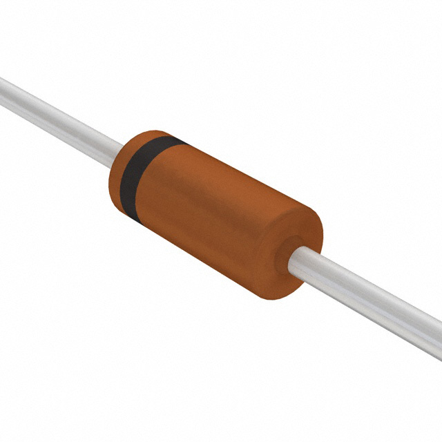


 工商网监
湘ICP备2023018690号
工商网监
湘ICP备2023018690号
