C6D10065E
Silicon Carbide Schottky Diode
Z-Rec®
Rectifier
Features
•
•
•
•
•
•
•
650 V
IF (TC=155˚C) =
10 A
Q c
34 nC
=
Package
New 6th Generation Technology
Low Forward Voltage Drop (VF)
Zero Reverse Recovery Current
Zero Forward Recovery Voltage
Low Leakage Current (Ir)
Temperature-Independent Switching Behavior
Positive Temperature Coefficient on VF
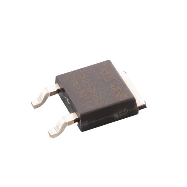
TO-252-2
Benefits
•
•
•
•
VRRM =
Higher System Level Efficiency
Increase System Power Density
Reduction of Heat Sink Requirements
Parallel Devices Without Thermal Runaway
PIN 1
CASE
PIN 2
Applications
•
•
•
•
•
Switch Mode Power Supplies (SMPS)
Server/Telecom Power Supplies
Industrial Power Supplies
Solar
UPS
Part Number
Package
Marking
C6D10065E
TO-252-2
C6D10065
Maximum Ratings (TC = 25˚C unless otherwise specified)
Symbol
Value Unit
Test Conditions
Note
VRRM
Repetitive Peak Reverse Voltage
650
V
VDC
DC Blocking Voltage
650
V
Continuous Forward Current
35
18
10
A
TC=25˚C
TC=125˚C
TC=155˚C
IFRM
Repetitive Peak Forward Surge Current
41
24
A
TC=25˚C, tP = 10 ms, Half Sine Wave
TC=110˚C, tP = 10 ms, Half Sine Wave
IFSM
Non-Repetitive Peak Forward Surge Current
78
68
A
TC=25˚C, tP = 10 ms, Half Sine Wave
TC=110˚C, tP = 10 ms, Half Sine Wave
Fig. 8
IF,Max
Non-Repetitive Peak Forward Surge Current
1100
1000
A
TC=25˚C, tP = 10 µs, Pulse
TC=110˚C, tP = 10 µs, Pulse
Fig. 8
99
43
W
TC=25˚C
TC=110˚C
Fig. 4
-55 to
+175
˚C
IF
Ptot
Power Dissipation
TJ , Tstg
1
Parameter
Operating Junction and Storage Temperature
C6D10065E Rev. A, 05-2020
Fig. 3
�Electrical Characteristics
Symbol
Parameter
Typ.
Max.
Unit
VF
Forward Voltage
1.27
1.37
1.50
1.60
V
IR
Reverse Current
2
15
50
200
QC
Total Capacitive Charge
C
EC
Test Conditions
Note
IF = 10 A TJ=25°C
IF = 10 A TJ=175°C
Fig. 1
μA
VR = 650 V TJ=25°C
VR = 650 V TJ=175°C
Fig. 2
34
nC
VR = 400 V, TJ = 25°C
Fig. 5
Total Capacitance
611
67
53
pF
VR = 0 V, TJ = 25°C, f = 1 MHz
VR = 200 V, TJ = 25˚C, f = 1 MHz
VR = 400 V, TJ = 25˚C, f = 1 MHz
Fig. 6
Capacitance Stored Energy
5.2
μJ
VR = 400 V
Fig. 7
Note: This is a majority carrier diode, so there is no reverse recovery charge.
Thermal Characteristics
Symbol
RθJC
Parameter
Typ.
Unit
Note
Thermal Resistance from Junction to Case
1.51
°C/W
Fig. 9
Typical Performance
100
20
18
14
mA)
IRI(Rm(A)
12
10
F F
Foward Current,
I I (A)
(A) IF (A)
16
Reverse Leakage Current, IRR (uA)
TJ = -55°C
TJ = 25°C
TJ = 75°C
TJ = 125°C
TJ = 175°C
8
6
4
2
0
0.50
0.75
1.00
1.25
1.50
Foward
(V) VF (V)
VVVoltage,
F(V)
F
Figure 1. Forward Characteristics
2
C6D10065E Rev. A, 05-2020
1.75
2.00
80
60
TJ = 175 °C
TJ = 125 °C
40
TJ = 75 °C
TJ = 25 °C
20
0
TJ = -55 °C
0
100
200
300
400
500
VV
(V)
Reverse
(V) VR (V)
R Voltage,
R
600
Figure 2. Reverse Characteristics
700
800
�Typical Performance
100
14
120
10% Duty
20% Duty
30% Duty
50% Duty
70% Duty
DC
100
12
80
10
70
(W)
P
(W)
PTot
(W)
PP
(W)
TOT
Tot
Tot
Tot
IF(peak)
(A)
IIF(peak)
(A)
(A)
I (A)
F(peak)
80
90
F
60
40
60
8
50
6
40
304
20
20
2
10
0
25
75
50
100
T
˚C
TTCCCC(°C)
˚C
T
˚C
125
150
0
175
25
Figure 3. Current Derating
12
50
Capacitance
CC(pF)
(pF)(pF)
256
C
C
CapacitiveQ
Charge,
QC (nC)
Q
C(nC)
(pF)
C (nC)
T
˚C
T
˚C
TCCCC(°C)
T
˚C
125
125
150
150
175
175
Conditions:
TJ = 25 °C
Ftest = 1 MHz
Vtest = 25 mV
160
600
20
4
15
10
2
5
140
500
120
400
100
80
300
60
200
40
100
20
0
100
200
300
400
500
(V) VR (V)
ReverseV
Voltage,
VV
(V)
R(V)
R
R
600
700
Figure 5. Total Capacitance Charge vs. Reverse Voltage
3
100
100
180
700
35
8
30
0
75
75
Figure 4. Power Derating
Conditions:
Conditions:
TJ = 25 °C
45
10
40
50
C6D10065E Rev. A, 05-2020
0
0
1
10
Reverse
VVoltage,
(V) VRR (V)
Reverse
R (V)
R
V
100
R
Figure 6. Capacitance vs. Reverse Voltage
1000
�Typical Performance
14
TJ_initial = 25 °C
TJ_initial = 110 °C
1,000
Capacitance Stored
ECEnergy,
(mJ) EC (mJ)
12
10
(A)
FSM(A)
IIFSM
8
6
100
4
2
0
0
100
200
300
400
500
ReverseVVoltage,
(V) VR (V)
600
10
10E-6
700
100E-6
Junction
To Case
Impedance,
ZthJC (oC/W)
Thermal
Resistance
(˚C/W)
Thermal
Resistance
(˚C/W)
Thermal
Resistance
(˚C/W)
Figure 7. Capacitance Stored Energy
Figure 8. Non-repetitive peak forward surge current
versus pulse duration (Sinusoidal Waveform)
0.5
0.3
0.1
100E-3
0.05
0.02
0.01
10E-3
1E-3
SinglePulse
1E-6
10E-6
100E-6
1E-3
Time,
tp (s)
(Sec)
T
TT(Sec)
(Sec)
10E-3
Figure 9. Transient Thermal Impedance
4
C6D10065E Rev. A, 05-2020
10E-3
Time,
tp (s)
tp (s)
R
1
1E-3
100E-3
1
�Package Dimensions
Package TO-252-2
SYMBOL
MILLIMETERS
MIN
MAX
A
2.159
2.413
A1
0
0.13
b
0.64
0.89
b2
0.653
1.143
b3
5.004
5.6
c
0.457
0.61
c2
0.457
0.864
D
5.867
6.248
D1
5.21
-
E
6.35
6.73
E1
4.32
e
Tjb June 2015
MX+DI+PSI
4.58 BSC
H
9.65
L
1.106
L2
10.414
1.78
0.51 BSC
L3
0.889
1.27
L4
0.64
1.01
Ɵ
0°
8°
Recommended Solder Pad Layout
TO-252-2
Part Number
Package
Marking
C6D10065E
TO-252-2
C6D10065
Note: Recommended soldering profiles can be found in the applications note here:
http://www.wolfspeed.com/power_app_notes/soldering
5
C6D10065E Rev. A, 05-2020
�Notes
• RoHS Compliance
The levels of RoHS restricted materials in this product are below the maximum concentration values (also referred
to as the threshold limits) permitted for such substances, or are used in an exempted application, in accordance
with EU Directive 2011/65/EC (RoHS2), as implemented January 2, 2013. RoHS Declarations for this product can
be obtained from your Wolfspeed representative or from the Product Ecology section of our website at http://
www.wolfspeed.com/power/tools-and-support/product-ecology.
• REACh Compliance
REACh substances of high concern (SVHCs) information is available for this product. Since the European Chemical Agency (ECHA) has published notice of their intent to frequently revise the SVHC listing for the foreseeable
future,please contact a Cree representative to insure you get the most up-to-date REACh SVHC Declaration.
REACh banned substance information (REACh Article 67) is also available upon request.
•
This product has not been designed or tested for use in, and is not intended for use in, applications implanted into
the human body nor in applications in which failure of the product could lead to death, personal injury or property
damage, including but not limited to equipment used in the operation of nuclear facilities, life-support machines,
cardiac defibrillators or similar emergency medical equipment, aircraft navigation or communication or control
systems, or air traffic control systems.
Related Links
•
•
•
Cree SiC Schottky diode portfolio: http://www.wolfspeed.com/Power/Products#SiCSchottkyDiodes
Schottky diode Spice models: http://www.wolfspeed.com/power/tools-and-support/DIODE-model-request2
SiC MOSFET and diode reference designs: http://go.pardot.com/l/101562/2015-07-31/349i
Copyright © 2020 Cree, Inc. All rights reserved.
The information in this document is subject to change without notice.
Cree, the Cree logo, and Zero Recovery are registered trademarks of Cree, Inc.
6
C6D10065E Rev. A, 05-2020
Cree, Inc.
4600 Silicon Drive
Durham, NC 27703
USA Tel: +1.919.313.5300
Fax: +1.919.313.5451
www.cree.com/power
�