CSD04060–Silicon Carbide Schottky Diode
Zero R
ecovery®
VRRM = 600 V
Rectifier
IF(AVG) = 4 A
Qc = 9 nC
Features
•
•
•
•
•
•
•
Package
600-Volt Schottky Rectifier
Zero Reverse Recovery Current
Zero Forward Recovery Voltage
High-Frequency Operation
Temperature-Independent Switching Behavior
Extremely Fast Switching
Positive Temperature Coefficient on VF
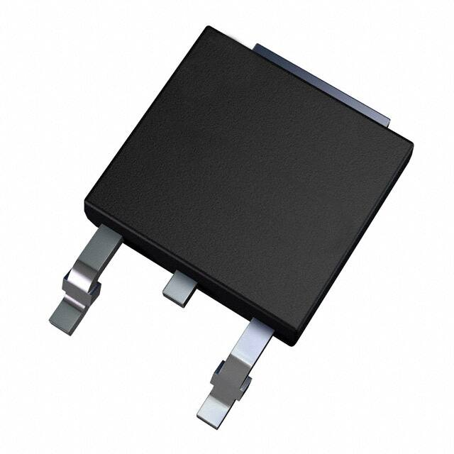
TO-252-2
TO-220-2
Benefits
•
•
•
•
•
Replace Bipolar with Unipolar Rectifiers
Essentially No Switching Losses
Higher Efficiency
Reduction of Heat Sink Requirements
Parallel Devices Without Thermal Runaway
PIN 1
CASE
PIN 2
Applications
•
•
•
Switch Mode Power Supplies
Power Factor Correction
- Typical PFC Pout : 400W-800W
Motor Drives
- Typical Power : 0.5HP-2HP
Part Number
Package
Marking
CSD04060A
TO-220-2
CSD04060
CSD04060E
TO-252-2
CSD04060
Maximum Ratings
Q
D04060 Rev.
Datasheet: CS
Symbol Parameter
Value
Unit
Test Conditions
VRRM
Repetitive Peak Reverse Voltage
600
V
VRSM
Surge Peak Reverse Voltage
600
V
VDC
DC Blocking Voltage
600
V
4
7
A
TC=150˚C
TC=125˚C
10
A
TC=125˚, TREP 1KHz
30% Duty
10
100
1000
VR Reverse Voltage (V)
10% Duty
Figure 3. Current Derating
Figure 4. Capacitance vs. Reverse Voltage
1.0E+01
Zth (°C/W)
1.0E+00
1.0E-01
1.0E-02
1.0E-03
1.E-07
1.E-06
1.E-05
1.E-04
1.E-03
Tim e (s)
Figure 5. Transient Thermal Impedance
3
CSD04060 Rev. Q
1.E-02
1.E-01
1.E+00
�Typical Performance
80.000
80
70
70.000
Power Dissipation (W)
60
60.000
50
50.000
40
40.000
30
30.000
20
20.000
10.000
10
0
0.000
25 50 75 100 125 150 175
25
50
75
100
125
150
175
TC Case Temperature (°C)
Figure 6. Power Derating
4
CSD04060 Rev. Q
�Package Dimensions
Inches
POS
Package TO-220-2
A
B
A
F
J
C
P
B
D
X
S
E
1 2
G
T
Z
L
M
W
N
PIN 1
CASE
PIN 2
9.677
10.414
.235.590 .255
.615
5.969
FC
D
.102.143 .112
2.591
.153
.337
.337
8.560
1.105
1.147
.590
.610
14.986
.500
.550
.149
.153
3.785
R1.147
0.19728.626
1.127
E
F
JG
V
.410
EB
LH
H
Max
.381
DA
H
U
Min
.255
5.969
M illim eters
.120
2.540
M in
M ax
.337
5.664
10.033 10.414
G
Y
Max
.235
Inc hes
.100
M in
M ax
.395.223 .410
C
P OS
Q
Millimeters
Min
14.986
6.477
6.477
3.048
8.560
15.621
2.845
3.632
3.886
8.560
28.067
29.134
15.494
12.700
13.970
3.886
R
0.197
29.134
MJ
L
N
M
PN
.530.025 .550
R 0.010
.045
.028
.036
.195
.045
.055
.195.165 .205
13.462 13.970
.036
.635
R 0.254
.055
1.143
.711
.914
.205
4.953
1.143
1.397
.185
4.191
4.953
5.207
QP
.170.048 .180
.054
4.318
1.219
4.572
1.372
SQ
S
T
T
U
U
VV
.048 3° .054
3°
5°
3°
3°
5°
3°
3°
5°
.100.094 .110
1.219
6°
3°
6°
3°
6°
3°
.110
2.54
1.3713°
5°
3°
5°
3°
5°
2.388
2.794
6°
WW
XX
.014.014 .021
3° 3° 5°
.356
.025
3°
5.5°
.533
.356
5° 3°
Y
z
Y
Z
.395
.410
.385
.130
.150
.130
10.033
.410
3.302
.150
10.414
9.779
3.810
3.302
.914
1.397
5.207
4.699
6°
6°
2.794
.635
5.5°
10.414
3.810
NOTE:
1. Dimension L, M, W apply for Solder Dip
Finish
Package Dimensions
Package TO-252-2
*
POS
Inches
Millimeters
Min
Max
Min
Max
A
.255
.265
6.477
6.731
B
.197
.205
5.004
5.207
C
.027
.033
.686
.838
D*
.270
.322
6.858
8.179
E
.178
.182
4.521
4.623
F
.025
.035
.635
.889
G
44˚
46˚
44˚
46˚
H
.382
.397
9.703
10.084
J
.090 TYP
2.286 TYP
K
6˚
8˚
6˚
8˚
L
.086
.094
2.184
2.388
M
.030
.034
.762
.864
N
.040
.044
1.016
1.118
P
.235
.245
5.969
6.223
Q
0.00
.004
0.00
.102
R
R0.01 TYP
.017
.023
.428
.588
T
.040
.044
1.016
1.118
U
.021
.027
.534
1.118
Note:
* Tab “D” may not be present
5
CSD04060 Rev. Q
R0.31 TYP
S
�Recommended Solder Pad Layout
.08
.26
TO-252-2
TO-220-2
Part Number
Package
Marking
CSD04060A
TO-220-2
CSD04060
CSD04060E
TO-252-2
CSD04060
Diode Model
Diode Model CSD04060
Vf T = VT + If*RT
VT= 0.965 + (Tj * -1.3*10-3)
RT= 0.096 + (Tj * 1.06*10-3)
Note: Tj = Diode Junction Temperature In Degrees Celcius
VT
RT
“The levels of environmentally sensitive, persistent biologically toxic (PBT), persistent organic pollutants (POP), or otherwise restricted materials in this product are below the
maximum concentration values (also referred to as the threshold limits) permitted for such substances, or are used in an exempted application, in accordance with EU Directive
2002/95/EC on the restriction of the use of certain hazardous substances in electrical and electronic equipment (RoHS), as amended through April 21, 2006. This part number was
released previously with Sn/Pb solder plating as a standard industry finish. For more information please contact power_sales@cree.com “
This product has not been designed or tested for use in, and is not intended for use in, applications implanted into the human body
nor in applications in which failure of the product could lead to death, personal injury or property damage, including but not limited
to equipment used in the operation of nuclear facilities, life-support machines, cardiac defibrillators or similar emergency medical
equipment, aircraft navigation or communication or control systems, air traffic control systems, or weapons systems.
Copyright © 2006-2009 Cree, Inc. All rights reserved. The information in this document is subject to change without notice. Cree,
the Cree logo, and Zero Recovery are registered trademarks of Cree, Inc.
6
CSD04060 Rev. Q
Cree, Inc.
4600 Silicon Drive
Durham, NC 27703
USA Tel: +1.919.313.5300
Fax: +1.919.313.5451
www.cree.com/power
�
很抱歉,暂时无法提供与“CSD04060E”相匹配的价格&库存,您可以联系我们找货
免费人工找货