OYLTDLJANF-27.000000 数据手册
OY Type Ultra Low Power
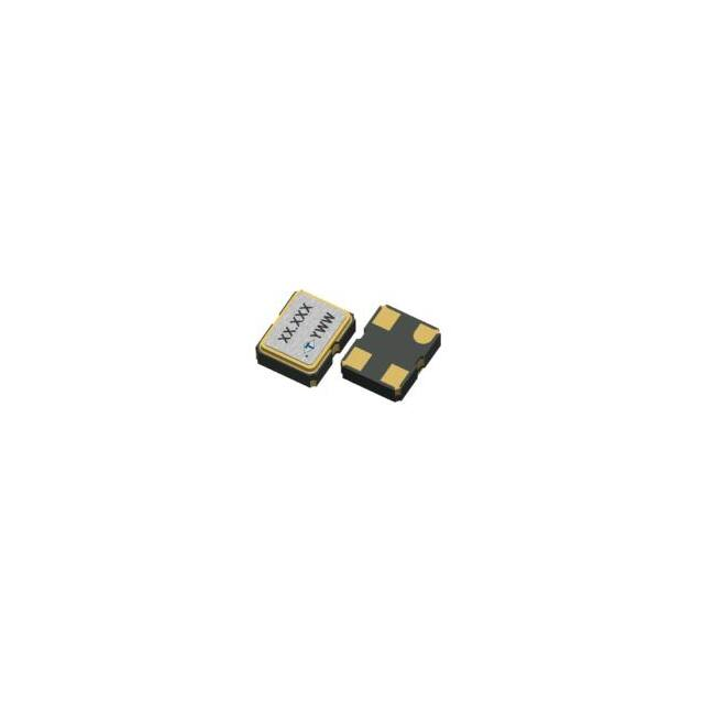
2.5 x 2.0mm SMD CMOS Output Crystal
Oscillator
Actual Size
FEATURE
- Ultra Low Power Supply Voltage: 0.9V, 1.2V, 1.5V Supply Options
- Singled-end Output: CMOS
- Frequency Support from 1MHz to 50MHz
- Low Noise Typical: 0.3ps at 12kHz to 20MHz Frequency Offsets
- Temperature Range: -40 to 85oC Operation
- Pb-free/RoHS Compliant
TYPICAL APPLICATION
- loT
- Game Console
- Smartphone
- Wearable Device
- Digital Camera - Digital Consumer Electronics
OY_PY
DIMENSION (mm)
SOLDER PAD L AYOUT (mm)
0.1 μF
[ B O T T O M V IE W ]
1.625 ± 0.10
#1
#1
0.675 ± 0.10 0.675
Pin#
0.81 ± 0.15
0.29
#4
#2
#2
[ S ID E V IE W ]
1
2
3
4
0.80
#3
0.57 ± 0.10
1.225 ± 0.10
#3
2.00 ± 0.20
2.50 ± 0.20
1.225
[ TO P VIEW ]
#4
RoHS Compliant
1.625
Function
0.90
Tri-state
GND
Output
VDD
Might cause malfunction if do not
To ensure optimal oscillator
place a by-pass capacitor of 0.1μF
followperformance,
the recommendation.
as close to the part as possible between Vdd and GND pads.
ELECTRICAL SPECIFICATION
0.9V
Parameter
Supply Voltage Variation (VDD)
Current
No Load Condition, 10MHz
Fo < 20MHz
No Load Condition, 20MHz
Fo < 50MHz
Max.
Min.
Max.
VDD+5%
VDD-5%
VDD+5%
V
1
50
1
50
1
50
MHz
-
1.5
-
2
-
3
mA
-
0.9
-
1
-
1.2
mA
-
1
-
1.2
-
1.2
mA
Fo < 10MHz
-
1.2
-
1.5
-
1.5
mA
45
55
45
55
45
55
%
Output High
2.97
-
2.25
-
1.62
-
V
Output Low
-
0.33
-
0.25
-
0.18
V
1MHz
-
4
-
3
-
3
nSec
Duty Cycle
Output Level
Transition Time:
Rise / Fall Time+
Fo < 10MHz
10MHz
Fo < 20MHz
-
3
-
3
-
3
nSec
20MHz
Fo < 50MHz
-
2
-
2
-
2
nSec
Startup Time
Enable (High Voltage or
Tri-State
Floating)
(Input to Pin 1)
Unit
Min.
VDD-5%
At 15pF Load
No Load Condition, 1MHz
1.5V
Max.
VDD+5%
Frequency Range
Supply
1.2V
Min.
VDD-5%
-
4
-
4
-
4
mSec
0.7xVDD
-
0.7xVDD
-
0.7xVDD
-
V
-
0.3xVDD
-
0.3xVDD
-
0.3xVDD
Disable (Low Voltage or GND)
Output Loading
15
15
15
Stand by Current
-
100
-
100
-
100
Aging (@ 25oC, 1st Year)
-
3
-
3
-
3
Storage Temp. Range
Phase Noise
V
pF
-55
+125
-55
+125
-55
+125
Typ.
Max.
Typ.
Max.
Typ.
Max.
-
A
ppm
o
C
1kHz offset
-130
-
-133
-
-135
At VDD=1.2V,
10kHz offset
-140
-
-143
-
-143
-
Fout=24MHz
100kHz offset
-148
-
-150
-
-150
-
1MHz offset
-152
-
-155
-
-155
-
Period Jitter (Pk-Pk)
-
40
-
40
-
40
pSec
RMS Phase Jitter (Integrated 12kHz to 20MHz)
-
1
-
1
-
1
pSec
dBc/Hz
Standard frequencies are frequencies which the crystal has been designed and does not imply a stock position
+Transition times are measured between 10% and 90% of VDD,withan output load of 15pF
FREQ. STABILITY vs. TEMP. RANGE
ppm
Temp.( oC)
-10~+60
-20~+70
-40~+85
25
50
* O: Available △:Conditional
X: Not available
*Inclusive of calibration @ 25℃, operating temperature range, input voltage variation,
load variation, aging (1st year), shock, and vibration load variation
Note: not all combination of options are available. Other specifications may be available upon request.
Specifications subject to change without notice.
www.taitien.com
sales@taitien.com.tw
Rev(2)08/2019
31
�
OYLTDLJANF-27.000000 价格&库存
很抱歉,暂时无法提供与“OYLTDLJANF-27.000000”相匹配的价格&库存,您可以联系我们找货
免费人工找货