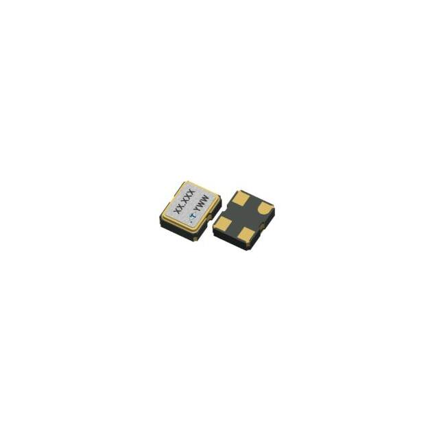
OYLTDLJANF-20.000000 数据手册
OX Type Ultra Low Power
3.2 x 2.5mm SMD CMOS Output Crystal
Oscillator
Actual Size
FEATURE
- Ultra Low Power Supply Voltage: 0.9V, 1.2V, 1.5V Supply Options
- Singled-end Output: CMOS
- Frequency Support from 1MHz to 50MHz
- Low Noise Typical: 0.3ps at 12kHz to 20MHz Frequency Offsets
- Temperature Range: -40 to 85oC Operation
- Pb-free/RoHS Compliant
RoHS Compliant
TYPICAL APPLICATION
- loT
- Game Console
- Smartphone
- Wearable Device
- Digital Camera - Digital Consumer Electronics
DIMENSION (mm)
SOLDER PAD L AYOUT (mm)
0.1 μF
[ B O T T O M V IE W ]
[ TO P VIEW ]
2.10 ± 0.15
1.65 ± 0.15
#2
#2
0.65 ± 0.15
#1
#4
#1
1.60
#3
#3
2.50 ± 0.15
#4
1.10
3.20 ± 0.15
2.10
0.90 ± 0.15
Pin#
0.35
0.95 ± 0.15
[ S ID E V IE W ]
1
2
3
4
Function
1.20
Tri-state
GND
Output
VDD
To ensure optimal oscillator performance, place a by-pass capacitor of 0.1μF
as close to the part as possible between Vdd and GND pads.
ELECTRICAL SPECIFICATION
0.9V
Parameter
Supply Voltage Variation (VDD)
Frequency Range
At 15pF Load
Fo < 10MHz
1.2V
1.5V
Unit
Min.
Max.
Min.
Max.
Min.
Max.
VDD-5%
VDD+5%
VDD-5%
VDD+5%
VDD-5%
VDD+5%
V
1
50
1
50
1
50
MHz
-
1.5
-
2
-
3
mA
-
0.9
-
1
-
1.2
mA
Supply
No Load Condition, 1MHz
Current
No Load Condition, 10MHz
Fo < 20MHz
-
1
-
1.2
-
1.2
mA
No Load Condition, 20MHz
Fo < 50MHz
-
1.2
-
1.5
-
1.5
mA
Duty Cycle
Output Level
Transition Time:
Rise / Fall Time+
45
55
45
55
45
55
%
Output High
2.97
-
2.25
-
1.62
-
V
Output Low
-
0.33
-
0.25
-
0.18
V
1MHz
-
4
-
3
-
3
nSec
Fo < 10MHz
10MHz
Fo < 20MHz
-
3
-
3
-
3
nSec
20MHz
Fo < 50MHz
-
2
-
2
-
2
nSec
Startup Time
Enable (High Voltage or
Tri-State
(Input to Pin 1)
Floating)
Disable (Low Voltage or GND)
-
4
-
4
-
4
mSec
0.7xVDD
-
0.7xVDD
-
0.7xVDD
-
V
-
0.3xVDD
-
0.3xVDD
-
0.3xVDD
Output Loading
15
15
15
Stand by Current
-
100
-
100
-
100
Aging (@ 25oC, 1st Year)
-
3
-
3
-
3
Storage Temp. Range
Phase Noise
V
pF
-55
+125
-55
+125
-55
+125
Typ.
Max.
Typ.
Max.
Typ.
Max.
A
ppm
o
C
1kHz offset
-130
-
-133
-
-135
-
At VDD=1.2V,
10kHz offset
-140
-
-143
-
-143
-
Fout=24MHz
100kHz offset
-148
-
-150
-
-150
-
1MHz offset
-152
-
-155
-
-155
-
Period Jitter (Pk-Pk)
-
40
-
40
-
40
pSec
RMS Phase Jitter (Integrated 12kHz to 20MHz)
-
1
-
1
-
1
pSec
dBc/Hz
Standard frequencies are frequencies which the crystal has been designed and does not imply a stock position
+Transition times are measured between 10% and 90% of VDD,withan output load of 15pF
FREQ. STABILITY vs. TEMP. RANGE
ppm
Temp.( oC)
-10~+60
-20~+70
-40~+85
25
50
* O: Available △:Conditional
X: Not available
*Inclusive of calibration @ 25℃, operating temperature range, input voltage variation,
load variation, aging (1st year), shock, and vibration load variation
Note: not all combination of options are available. Other specifications may be available upon request.
Specifications subject to change without notice.
www.taitien.com
sales@taitien.com.tw
Rev(2)08/2019
33
�
OYLTDLJANF-20.000000 价格&库存
很抱歉,暂时无法提供与“OYLTDLJANF-20.000000”相匹配的价格&库存,您可以联系我们找货
免费人工找货