PJM7002KNDC
N-Channel Enhancement Mode Power MOSFET
Features
DFN1x0.6-3L
⚫ Fast switching
3.D
⚫ Low gate charge and RDS(ON)
⚫ Low reverse transfer capacitances
⚫ VDS= 60V,ID= 0.3A
1.G
2.S
RDS(on)< 3Ω @VGS= 10V
Marking Code: K72
Schematic Diagram
Applications
⚫ Load switch
3.Drain
⚫ PWM application
1.Gate
2.Source
Absolute Maximum Ratings
Ratings at 25℃ ambient temperature unless otherwise specified.
Parameter
Symbol
Value
Unit
Drain-Source Voltage
VDS
60
V
Gate-Source Voltage
VGS
±20
V
Drain Current-Continuous
ID
0.3
A
Drain Current-Pulsed Note1
IDM
0.8
A
Maximum Power Dissipation
PD
0.3
W
Junction Temperature
TJ
150
°C
TSTG
-55 to +150
°C
RθJA
357
°C/W
Storage Temperature Range
Thermal Characteristics
Thermal Resistance,Junction-to-Ambient Note2
www.pingjingsemi.com
Revision:2.0 Aug-2021
1/5
�PJM7002KNDC
N-Channel Enhancement Mode Power MOSFET
Electrical Characteristics
(Ta=25℃ unless otherwise specified)
Parameter
Symbol
Test Condition
Min.
Typ.
Max.
Unit
Drain-Source Breakdown Voltage
V(BR)DSS
VGS=0V,ID=250μA
60
--
--
V
Zero Gate Voltage Drain Current
IDSS
VDS=60V,VGS=0V
--
--
1
μA
Gate-Body Leakage Current
IGSS
VGS=±20V,VDS=0V
--
--
±10
μA
Gate Threshold Voltage Note3
VGS(th)
VDS=VGS,ID=250μA
1
1.4
2.5
V
Drain-Source On-Resistance Note3
RDS(on)
VGS=10V,ID=0.5A
--
1.9
3
Ω
VGS=4.5V,ID=0.3A
--
2.2
4
Ω
VDS=10V,ID=0.2A
0.1
--
--
S
--
21
--
pF
--
11
--
pF
Static Characteristics
Forward Transconductance Note3
gFS
Dynamic Characteristics
Input Capacitance
Ciss
Output Capacitance
Coss
Reverse Transfer Capacitance
Crss
--
4.2
--
pF
Turn-on Delay Time
td(on)
--
10
--
nS
Turn-on Rise Time
tr
VDS=30V, ID=0.2A
--
50
--
nS
Turn-off Delay Time
td(off)
VGEN=10V,RG=10Ω
--
17
--
nS
--
10
--
nS
VDS=25V,VGS=0V,f=1MHz
Switching Characteristics
Turn-off Fall Time
tf
Total Gate Charge
Qg
VDS=10V,ID=0.3A, VGS=4.5V
--
1.7
--
nC
Diode Forward Voltage Note3
VSD
VGS=0V,IS=0.2A
--
--
1.2
V
Diode Forward Current Note2
IS
--
--
0.3
A
Source-Drain Diode Characteristics
Note: 1. Repetitive Rating: Pulse width limited by maximum junction temperature.
2. Surface Mounted on FR4 Board, t ≤ 10 sec.
3. Pulse Test: Pulse width≤300μs, duty cycle≤2%.
www.pingjingsemi.com
Revision:2.0 Aug-2021
2/5
�PJM7002KNDC
N-Channel Enhancement Mode Power MOSFET
ID Drain Current (A)
RDS(on) On-Resistance(Ω)
Typical Characteristic Curves
VDS Drain-Source Voltage (V)
ID Drain Current (A)
Normalized On-Resistance
ID Drain Current (A)
TJ Junction Temperature(℃)
C Capacitance (pF)
RDS(on) On-Resistance(Ω)
VGS Gate-Source Voltage (V)
VGS Gate-Source Voltage (V)
www.pingjingsemi.com
Revision:2.0 Aug-2021
VDS Drain-Source Voltage (V)
3/5
�VGS Gate-Source Voltage (V)
IS Reverse Drain Current (A)
PJM7002KNDC
N-Channel Enhancement Mode Power MOSFET
VSD Source-Drain Voltage (V)
r(t),Normalized Effective
Transient Thermal Impedance
Qg Gate Charge (nC)
Square Wave Pluse Duration(sec)
www.pingjingsemi.com
Revision:2.0 Aug-2021
4/5
�PJM7002KNDC
N-Channel Enhancement Mode Power MOSFET
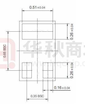
Package Outline
DFN1x0.6-3L-0009
Dimensions in mm
Ordering Information
Device
Package
PJM7002KNDC
DFN1x0.6-3L
www.pingjingsemi.com
Revision:2.0 Aug-2021
Shipping
10,000PCS/Reel&7inches
5/5
�
很抱歉,暂时无法提供与“PJM7002KNDC”相匹配的价格&库存,您可以联系我们找货
免费人工找货- 国内价格
- 50+0.07650
- 500+0.06885
- 5000+0.06375
- 10000+0.06120
- 30000+0.05865
- 50000+0.05712
- 国内价格
- 20+0.11425
- 200+0.08975
- 600+0.07614
- 2000+0.06798
- 10000+0.05463
- 20000+0.05081