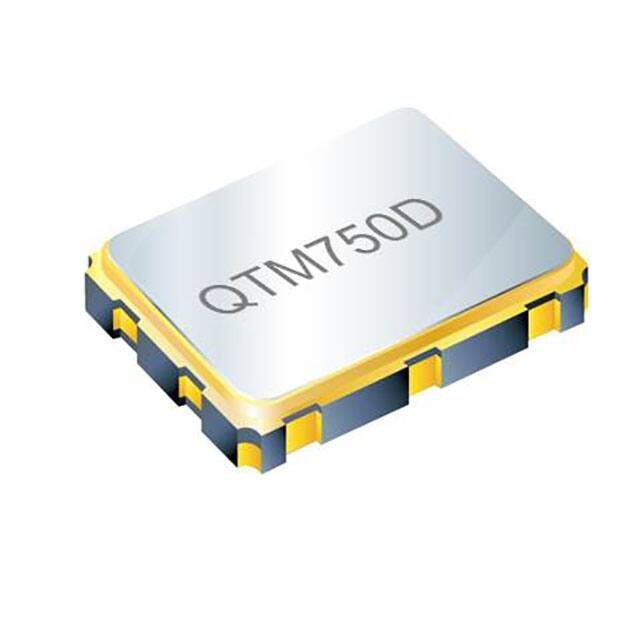
QTM750D-125.000MCE-T 数据手册
QTM750D
MHz LVDS Oscillator
Fuel The Digital World
Features
●
●
●
●
●
●
●
●
Applications
Frequency range : 25MHz to 312.5MHz
SMD seam sealing ceramic package
Supply voltage : 2.5V, 3.3V
LVDS output
Low phase noise and phase jitter
Tri-state function available
External dimensions (mm)
L : 7.0 x W : 5.0 x H : 1.4
RoHS compliant & Pb free
●
●
●
●
●
Networking, Telecommunication,
Data communication, Switch,
Server, Storage
Fibre channel, Ethernet, SONET,
SATA, SAS, PCI-Express
Optical module
Microprocessor, DSP, FPGA,
Clock source for ADC and DAC
Test and measurement
Electrical Characteristics
Item
Frequency Range (F0)
Frequency Stability (Fstab) over
Operating Temperature Range (T OTR)
Operating Temperature Range (T OTR)
Supply Voltage (VDD)
Current Consumption (IDD)
QTM750D
25MHz ~ 312.5MHz
±50ppm, ±25ppm
-40°C ~ +85°C, Note [1]
±50ppm
-40°C ~ +105°C, Note [1]
-40°C ~ +85°C
-40°C ~ +105°C
2.5V, 3.3V
LVDS
Output Load
100 Ω
Output Voltage High (VOH)
1.43V Typ. / 1.6V Max.
Output Voltage Low (VOL)
0.9V Min. / 1.1V Typ.
Offset Voltage
1.125V Min. / 1.25V Typ. / 1.375V Max.
Differential Output Voltage
247mV Min. / 330mV Typ. / 454mV Max.
Rise & Fall Time (Tr / Tf)
0.6 ns Max.
Duty Cycle
45% ~ 55%
Start-up Time
5 ms Max.
Enable Voltage High, Logic "1"
70% VDD Min.
Enable Voltage Low, Logic "0"
30% VDD Max.
F0 = 156.25MHz
F0 = 312.5MHz
Aging (Faging)
Storage Temperature Range (TSTR)
Rev. 1.01
VDD ± 10%
50 mA Max.
Output Type
Phase Jitter
Conditions
20%~80% of output swing
Input to OE pin
Note [2]
150fs ~ 300fs Max.
80fs Typ. / 100fs Max.
12kHz ~ 20MHz, RMS
±3 ppm Max.
at 25°C±3°C, first year
-55°C ~ +125°C
Page 1
www.qstproducts.com
�QTM750D
MHz LVDS Oscillator
Fuel The Digital World
Notes:
[1] Inclusive of frequency tolerance at 25°C, variations over temperature, supply voltage and vibration.
[2] Output will be enabled if OE is Logic "1" or Open; Output will be disabled if OE is Logic "0".
[3] The standard testing environment except temperature test is 25°C±5°C, 40%~70% relative humidity.
Dimensions
Pin function
Pin 1
OE
Pin 2
NC
Pin 3
GND
Pin 4
OUT
Pin 5
OUT
VDD
Pin 6
Recommended pad layout
(Unit: mm)
* Pad dimension tolerance is ±0.2mm
* Power supply decoupling capacitor is required.
Ordering Information
QTM750D -
156.25M B
E
Frequency in Hz
-
T
Packaging Method
T
Please contact us for
available frequencies
Tape & Reel
Frequency Stability
Supply Voltage
B
C
Rev. 1.01
E
D
G
3.3 V
2.5 V
Page 2
± 50 ppm ( -40°C ~ +85°C )
± 25 ppm ( -40°C ~ +85°C )
± 50 ppm ( -40°C ~ +105°C )
www.qstproducts.com
�QTM750D
MHz LVDS Oscillator
Fuel The Digital World
Packing
(Unit: mm)
Reflow Profile
Solder melting point : 220°C ± 10°C, 60 sec. Min., 200 sec. Max.
Peak temperature : 260°C ± 10°C, 10 sec. Min., 30 sec. Max.
(°C)
10 sec
260
220
180
150
120 sec
Rev. 1.01
60 sec
Page 3
Time (sec)
www.qstproducts.com
�
QTM750D-125.000MCE-T 价格&库存
很抱歉,暂时无法提供与“QTM750D-125.000MCE-T”相匹配的价格&库存,您可以联系我们找货
免费人工找货