SIT8021AI-J4-18S-19.200000 数据手册
SiT8021
1 to 26 MHz, Ultra-Small µPower Oscillator
Description
Features
The SiT8021 is the industry's smallest and the lowest
power MHz oscillator. With 0.1 mW of active power
consumption at 3.072 MHz output frequency, this µPower
oscillator enables longer battery life for a wearable, IoT or
mobile device compared to a quartz-based oscillator or
resonator.
Ultra-low current consumption of 60 µA at 3.072 MHz
Ultra-small 1.5 mm x 0.8 mm package
1 to 26 MHz with 6 decimal places of accuracy
Operating temperature from -40°C to 85°C
Frequency stability as low as ±100 ppm
Programmable output drive strength for best EMI or
driving multiple loads
Ultra-light weight of 1.28 mg
RoHS and REACH compliant, Pb-free, Halogen-free
and Antimony-free
The device comes in the smallest 1.5 mm x 0.8 mm
package. The unique combination of ultra-low power, ultrasmall package and flexible output frequency makes it ideal
for power sensitive and space constrained applications.
Applications
Tablets
Fitness bands
Health and medical monitoring
Wearables
Portable audio
Input devices
IoT devices
Electrical Specifications
Table 1. Electrical Characteristics
All Min and Max limits are specified over temperature and rated operating voltage with 15 pF output load unless otherwise
stated. Typical values are at 25°C and nominal supply voltage.
Parameters
Symbol
Min.
Typ.
Max.
Unit
Condition
Frequency Range
Output Frequency Range
f
1.000000
26.000000
MHz
Frequency Stability and Aging
Initial Tolerance
Frequency Stability
First Year Aging
f_tol
-15
–
+15
ppm
Frequency offset at 25°C post reflow
f_stab
-100
–
+100
ppm
Inclusive of initial tolerance, and variations over operating
temperature, rated power supply voltage and output load.
Contact SiTime for ±25 or ±50 ppm options.
f_1year
-3
+3
ppm
at 25°C
Operating Temperature Range
Operating Temperature Range
T_use
-20
–
+70
°C
Extended Commercial
-40
–
+85
°C
Industrial. Contact SiTime for -40°C to 105°C option.
Supply Voltage and Current Consumption
Supply Voltage
Current Consumption[1,3]
Standby Current[3]
Rev 1.2
VDD
IDD
I_std
1.62
1.8
1.98
2.25
–
3.63
V
Any voltage from 2.25 to 3.63V
–
60
–
µA
f = 3.072 MHz, Vdd = 1.8V, no load
–
110
130
µA
f = 6.144 MHz, Vdd = 1.8V, no load
–
230
270
µA
f = 6.144 MHz, Vdd = 1.8V, 10 pF load
–
–
160
µA
f = 6.144 MHz, Vdd = 2.25V to 3.63V, no load
–
160
–
µA
f = 12 MHz, Vdd = 1.8V, no load
–
0.7
1.3
µA
Vdd = 1.8V, ST pin = HIGH, output is weakly pulled down
–
–
1.5
µA
Vdd = 2.25V to 3.63V, ST pin = HIGH, output is weakly
pulled down
September 28, 2017
V
www.sitime.com
�SiT8021 1 to 26 MHz, Ultra-Small µPower Oscillator
Table 1. Electrical Characteristics (continuous)
Parameters
Symbol
Min.
Typ.
Max.
Unit
Condition
LVCMOS Output Characteristics
Duty Cycle
DC
Rise/Fall Time[3]
45
–
55
%
–
4
8
ns
Vdd = 1.8V, 20% - 80%. Contact SiTime for other
programmable rise/fall options
–
–
8
ns
Vdd = 2.25V to 3.63V, 20% - 80%. Contact SiTime for other
programmable rise/fall options
90%
–
–
VDD
IOH = -0.5 mA (Vdd = 1.8V)
IOH = -1.2 mA (Vdd = 2.25V to 3.63V)
–
–
10%
VDD
IOL = 0.5 mA (Vdd = 1.8V)
IOL = 1.2 mA (Vdd = 2.25V to 3.63V)
T_r, T_f
Output High Voltage
VOH
Output Low Voltage
VOL
Input High Voltage
VIH
80%
–
–
VDD
Input Low Voltage
VIL
–
–
20%
VDD
Input Slew Rate
In-slew
10
–
–
V/µs
Input Pull-down Impedance
Z_in
300
–
–
kΩ
Active mode (ST pin = LOW), Vdd = 1.8V
270
–
–
kΩ
Active mode (ST pin = LOW), Vdd = 2.25V to 3.63V
2.5
–
–
MΩ
Standby mode (ST pin = HIGH), Vdd = 1.8V
1.3
–
–
MΩ
Standby mode (ST pin = HIGH), Vdd = 2.25V to 3.63V
Input Characteristics
Startup, Standby and Resume Timing
Startup Time
T_start
–
75
150
ms
Measured from the time VDD reaches 90% of its final value
Standby Time
T_stdby
–
–
20
µs
Measured from the time ST pin crosses 50% threshold
Resume Time
T_resume
–
2
3
ms
Measured from the time ST pin crosses 50% threshold
Jitter
RMS Period Jitter[3]
T_jitt
RMS Phase Jitter[3]
T_phj
–
75
110
ps
f = 6.144 MHz, Vdd = 1.8V
–
–
110
ps
f = 6.144 MHz, Vdd = 2.25V to 3.63V
–
0.8
2.5
ns
f = 6.144 MHz, Vdd = 1.8V,
Integration bandwidth = 100 Hz to 40 kHz[2]
–
–
2.5
ns
f = 6.144 MHz, Vdd = 2.25V to 3.63V,
Integration bandwidth = 100 Hz to 40 kHz[2]
Notes:
1. Current consumption with load is a function of the output frequency and output load. For any given output frequency, the capacitive loading will increase
current consumption equal to C_load*VDD*f(MHz).
2. Max spec inclusive of 25 mV peak-to-peak sinusoidal noise on VDD. Noise frequency 100 Hz to 20 MHz.
3. Refer to the performance plot section for typical values at 2.5, 2.8, 3.0 and 3.3V condition
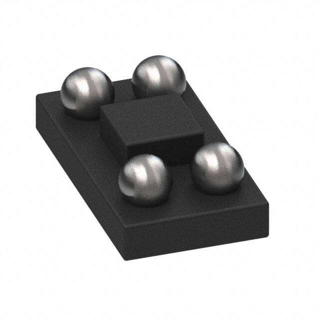
Top View
Table 2. Pin Description
Pin
Symbol
Functionality
L: Specified frequency output
1
ST
Input
2
OUT
Output
LVCMOS clock output
3
VDD
Power
Supply voltage. Bypass with a 0.01µF X7R capacitor.
4
GND
Power
Connect to ground
Rev 1.2
ST
1
4
GND
OUT
2
3
VDD
H: Output is low (weak pull down). Device goes to the standby mode.
Supply current reduces to I_std.
Figure 1. Pin Assignments
Page 2 of 10
www.sitime.com
�SiT8021 1 to 26 MHz, Ultra-Small µPower Oscillator
Table 3. Absolute Maximum Limits
Attempted operation outside the absolute maximum ratings may cause permanent damage to the part.
Actual performance of the IC is only guaranteed within the operational specifications, not at absolute maximum ratings.
Parameter
Test Condition
Continuous Power Supply Voltage Range (VDD)
Short Duration Maximum Power Supply Voltage (VDD)
Value
Unit
-0.5 to 3.63
V
SIT8021AI-J4-18S-19.200000 价格&库存
很抱歉,暂时无法提供与“SIT8021AI-J4-18S-19.200000”相匹配的价格&库存,您可以联系我们找货
免费人工找货- 国内价格 香港价格
- 1+11.329271+1.46735
- 国内价格
- 1+7.13880
- 200+2.85120
- 500+2.75400
- 1000+2.71080