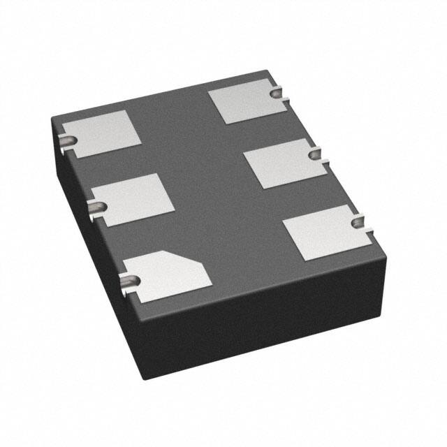
SiT9366
1 MHz to 220 MHz Ultra-low Jitter Differential Oscillator
Description
The SiT9366 is a 1 MHz to 220 MHz differential MEMS
XO engineered for low-jitter applications. Utilizing
SiTime’s unique DualMEMS® temperature sensing and
TurboCompensation® technology, the SiT9366 delivers
exceptional dynamic performance by providing
resistance to airflow, thermal gradients, shock and
vibration. This device also integrates multiple on-chip
regulators to filter power supply noise, eliminating the
need for a dedicated external LDO.
The SiT9366 can be factory programmed for any
combination of frequency, stability, voltage, and output
signaling. Programmability enables designers to optimize
clock configurations while eliminating long lead times and
customization costs associated with quartz devices
where each frequency is custom built.
The wide frequency range and programmability makes
this device ideal for telecom, networking, and industrial
applications that require a variety of frequencies and
operate in noisy environments.
Features
Any frequency between 1 MHz and 220 MHz accurate to
6 decimal places
(For additional frequencies, refer to SiT9367 and SiT9365
datasheets)
LVPECL, Low-swing LVPECL, LVDS and HCSL
output signaling
0.1 ps RMS phase jitter (random) for Ethernet applications
Frequency stability as low ±10 ppm
Wide temperature ranges from -40°C to 105°C
Industry-standard packages: 7.0 x 5.0 mm2, 5.0 x 3.2 mm2,
3.2 x 2.5 mm2 packages
Applications
10/40/100 Gbps Ethernet, SONET, SATA, SAS,
Fibre Channel
Telecom, networking, instrumentation, storage, servers
Refer to Manufacturing Notes for proper reflow profile,
tape and reel dimension, and other manufacturing
related information.
Block Diagram
Package Pinout
Figure 1. SiT9366 Block Diagram
Rev 1.09
OE/NC
1
6
VDD
NC
2
5
OUT-
GND
3
4
OUT+
Figure 2. Pin Assignments (Top view)
(Refer to Table 6 for Pin Descriptions)
20 July 2021
www.sitime.com
�SiT9366 1 MHz to 220 MHz Ultra-low Jitter Differential Oscillator
Ordering Information
SiT9366AC - 1B2-33E125.000000T
Part Family
Packaging
“SiT9366”
“T”, “Y”, “D” or “E”
Refer to table below for packing method
[1]
Leave Blank for Bulk
Revision Letter
“A” is the revision of Silicon
Frequency
1.000000 to 220.000000 MHz
Temperature Range
“C”: Extended Commercial, -20 to 70°C
“I”: Industrial, -40 to 85°C
“B”: -40 to 95°C
“E”: Extended Industrial, -40 to 105°C
Feature Pin
“N”: No Connect
“E”: Output Enable
Signalling Type
“1”:
“2”:
“4”:
“5”:
Voltage Supply
LVPECL
LVDS
HCSL
Low-swing LVPECL
“25”: 2.5 V ±10%
“28”: 2.8 V ±10%
“30”: 3.0 V ±10%
“33”: 3.3 V ±10%
Package Size
“B”: 3.2 x 2.5 mm
“C”: 5.0 x 3.2 mm with center pad
“E”: 7.0 x 5.0 mm with center pad
Frequency Stability
“F”:
“1”:
“2”:
“3”:
±10 ppm
±20 ppm
±25 ppm
±50 ppm
Notes:
1. Bulk is available for sampling only
Table 1. Ordering Codes for Supported Tape & Reel Packing Method
Device Size
(mm x mm)
8 mm T&R
(3ku)
8 mm T&R
(1ku)
12 mm T&R
(3ku)
12 mm T&R
(1ku)
16 mm T&R
(3ku)
16 mm T&R
(1ku)
7.0 x 5.0
—
—
—
—
T
Y
T
Y
—
—
5.0 x 3.2
3.2 x 2.5
Rev 1.09
D
E
Page 2 of 16
www.sitime.com
�SiT9366 1 MHz to 220 MHz Ultra-low Jitter Differential Oscillator
TABLE OF CONTENTS
Description ................................................................................................................................................................................... 1
Features ....................................................................................................................................................................................... 1
Applications .................................................................................................................................................................................. 1
Block Diagram .............................................................................................................................................................................. 1
Package Pinout ............................................................................................................................................................................ 1
Ordering Information .................................................................................................................................................................... 2
Electrical Characteristics .............................................................................................................................................................. 4
Waveform Diagrams..................................................................................................................................................................... 9
Timing Diagrams ........................................................................................................................................................................ 10
Termination Diagrams ................................................................................................................................................................ 11
LVPECL and Low-swing LVPECL ....................................................................................................................................... 11
LVDS................................................................................................................................................................................... 12
HCSL .................................................................................................................................................................................. 12
Dimensions and Patterns ― 3.2 x 2.5 mm2................................................................................................................................ 13
Dimensions and Patterns ― 5.0 x 3.2 mm2................................................................................................................................ 13
Dimensions and Patterns ― 7.0 x 5.0 mm2................................................................................................................................ 14
Additional Information................................................................................................................................................................. 15
Revision History ......................................................................................................................................................................... 15
Rev 1.09
Page 3 of 16
www.sitime.com
�SiT9366 1 MHz to 220 MHz Ultra-low Jitter Differential Oscillator
Electrical Characteristics
All Min and Max limits in the Electrical Characteristics tables are specified over temperature and rated operating voltage with standard
output termination show in the termination diagrams. Typical values are at 25°C and nominal supply voltage.
Table 2. Electrical Characteristics – Common to LVPECL, Low-swing LVPECL, LVDS and HCSL (All
temperature ranges)
Parameter
Symbol
Min.
Typ.
Max.
Unit
Condition
Frequency Range
Output Frequency Range
f
1
–
220.000001
MHz
Accurate to 6 decimal places
Frequency Stability
Frequency Stability
F_stab
-10
–
+10
ppm
-20
–
+20
ppm
-25
–
+25
ppm
-50
–
+50
ppm
Inclusive of initial tolerance, operating temperature, rated power
supply voltage and load variations
First Year Aging
F_1y
-0.7
±0.4
+0.7
ppm
At 85°C
5 Year Aging
F_5y
-1.1
±0.7
+1.1
ppm
At 85°C
10 Year Aging
F_10y
-1.3
±0.8
+1.3
ppm
At 85°C
20 Year Aging
F_20y
-1.5
±1.0
+1.5
ppm
At 85°C
Operating Temperature Range
T_use
-20
–
-40
–
-40
–
-40
–
Temperature Range
+70
°C
Extended Commercial
+85
°C
Industrial
+95
°C
+105
°C
Extended Industrial
Supply Voltage
Supply Voltage
Vdd
2.97
3.30
3.63
V
2.70
3.00
3.30
V
2.52
2.80
3.08
V
2.25
2.50
2.75
V
Input Characteristics
Input Voltage High
VIH
70%
–
–
Vdd
Pin 1, OE
Input Voltage Low
VIL
–
–
30%
Vdd
Pin 1, OE
Input Pull-up Impedance
Z_in
–
100
-
kΩ
Pin 1, OE logic high or logic low
Output Characteristics
Duty Cycle
DC
45
–
55
%
Startup and OE Timing
Startup Time
OE Enable/Disable Time
Rev 1.09
T_start
T_oe
–
–
–
–
3.0
ms
Measured from the time Vdd reaches its rated minimum value.
3.8
µs
f = 156.25 MHz. Measured from the time OE pin reaches rated
VIH and VIL to the time clock pins reach 90% of swing and
high-Z. See Figure 8 and Figure 9.
Page 4 of 16
www.sitime.com
�SiT9366 1 MHz to 220 MHz Ultra-low Jitter Differential Oscillator
Table 3. Electrical Characteristics – LVPECL, Low-swing LVPECL
Parameter
Symbol
Min.
Typ.
Max.
Unit
Condition
Current Consumption
Current Consumption
Idd
–
–
89
mA
OE Disable Supply Current
I_OE
–
–
58
mA
OE = Low
Output Disable Leakage
Current
I_leak
–
0.15
–
µA
OE = Low
I_driver
–
–
32
mA
Maximum average current drawn from OUT+ or OUT-
Maximum Output Current
Excluding Load Termination Current, Vdd = 3.3 V or 2.5 V
Output Characteristics for LVPECL
Output High Voltage
VOH
Vdd-1.1
–
Vdd-0.7
V
See Figure 4
Output Low Voltage
VOL
Vdd-1.9
–
Vdd-1.5
V
See Figure 4
V_Swing
1.2
1.6
2.0
V
See Figure 5
Tr, Tf
–
225
290
ps
20% to 80%, See Figure 5
Output Differential Voltage
Swing
Rise/Fall Time
Output High Voltage
Output Low Voltage
Output Differential Voltage
Swing
VOH
Output Characteristics for Low-swing LVPECL
–
Vdd-1.2
Vdd-0.75
V
See Figure 4
VOL
Vdd-1.8
–
Vdd-1.25
V
See Figure 4
V_Swing
0.4
1
1.2
V
Output frequency 1 to 220 MHz, See Figure 5
0.4
1
1.6
V
Output frequency greater than 220 MHz, See Figure 5
225
290
ps
20% to 80%. See Figure 5
Rise/Fall Time
Tr, Tf
–
RMS Period Jitter[2]
T_jitt
–
1.0
1.6
ps
f = 100, 156.25 or 212.5 MHz, Vdd = 3.3 V or 2.5 V
RMS Phase Jitter (random)
T_phj
–
0.225
0.270
ps
f = 156.25 MHz, Integration bandwidth = 12 kHz to 20 MHz,
all Vdd levels, includes spurs. Temperature ranges -20 to
70ºC and -40 to 85ºC
–
0.225
0.300
ps
f = 156.25 MHz, Integration bandwidth = 12 kHz to 20 MHz,
all Vdd levels, includes spurs. Temperature ranges -40 to
95ºC and -40 to 105ºC
–
0.1
–
ps
f = 156.25 or 322.265625 MHz, IEEE802.3-2005 10GbE jitter
mask integration bandwidth = 1.875 MHz to 20 MHz, includes
spurs, all Vdd levels.
Jitter – 7.0 x 5.0 mm Package
Jitter – 5.0 x 3.2 and 3.2 x 2.5 mm Packages
RMS Period Jitter[2]
T_jitt
RMS Phase Jitter (random)
–
1.0
1.6
ps
f = 100, 156.25 or 212.5 MHz, Vdd = 3.3 V or 2.5 V
–
0.225
0.275
ps
f = 156.25 MHz, Integration bandwidth = 12 kHz to 20 MHz,
all Vdd levels, includes spurs. Temperature ranges -20 to
70ºC and -40 to 85ºC
–
0.225
0.340
ps
f = 156.25 MHz, Integration bandwidth = 12 kHz to 20 MHz,
all Vdd levels, includes spurs. Temperature ranges -40 to
95ºC and -40 to 105ºC
–
0.1
–
ps
f = 156.25 or 322.265625 MHz, IEEE802.3-2005 10GbE jitter
mask integration bandwidth = 1.875 MHz to 20 MHz, includes
spurs, all Vdd levels.
Notes:
2. Measured according to JESD65B.
Rev 1.09
Page 5 of 16
www.sitime.com
�SiT9366 1 MHz to 220 MHz Ultra-low Jitter Differential Oscillator
Table 4. Electrical Characteristics – LVDS
Parameter
Symbol
Min.
Typ.
Max.
Unit
Condition
Current Consumption
Current Consumption
Idd
–
–
79
mA
OE Disable Supply Current
I_OE
–
–
58
mA
Excluding Load Termination Current, Vdd = 3.3 V or 2.5 V
OE = Low
Output Disable Leakage
Current
I_leak
–
0.15
–
µA
OE = Low
Differential Output Voltage
VOD
300
–
450
mV
See Figure 6
ΔVOD
–
–
50
mV
See Figure 6
VOS
1.125
–
1.375
V
See Figure 6
Delta VOS
ΔVOS
–
–
50
mV
See Figure 6
Rise/Fall Time
Tr, Tf
–
400
470
ps
Measured with 2 pF capacitive loading to GND, 20% to 80%,
see Figure 7
RMS Period Jitter[3]
T_jitt
1.0
1.6
ps
f = 100, 156.25 or 212.5 MHz, Vdd = 3.3 V or 2.5 V
RMS Phase Jitter (random)
T_phj
–
–
0.215
0.265
ps
f = 156.25 MHz, Integration bandwidth = 12 kHz to 20 MHz,
all Vdd levels, includes spurs. Temperature ranges -20 to
70ºC and -40 to 85ºC
–
0.215
0.300
ps
–
f = 156.25 MHz, Integration bandwidth = 12 kHz to 20 MHz,
all Vdd levels, includes spurs. Temperature ranges -40 to
95ºC and -40 to 105ºC
0.1
–
ps
f = 156.25 or 322.265625 MHz, IEEE802.3-2005 10GbE jitter
mask integration bandwidth = 1.875 MHz to 20 MHz, includes
spurs, all Vdd levels.
Output Characteristics
Delta VOD
Offset Voltage
Jitter – 7.0 x 5.0 mm Package
Jitter – 5.0 x 3.2 and 3.2 x 2.5 mm Packages
RMS Period Jitter[3]
T_jitt
RMS Phase Jitter (random)
T_phj
–
–
1.0
1.6
ps
f = 100, 156.25 or 212.5 MHz, Vdd = 3.3 V or 2.5 V
0.235
0.275
ps
f = 156.25 MHz, Integration bandwidth = 12 kHz to 20 MHz,
all Vdd levels, includes spurs. Temperature ranges -20 to
70ºC and -40 to 85ºC
–
0.235
0.320
ps
f = 156.25 MHz, Integration bandwidth = 12 kHz to 20 MHz,
all Vdd levels, includes spurs. Temperature ranges -40 to
95ºC and -40 to 105ºC
–
0.1
–
ps
f = 156.25 or 322.265625 MHz, IEEE802.3-2005 10GbE jitter
mask integration bandwidth = 1.875 MHz to 20 MHz, includes
spurs, all Vdd levels.
Notes:
3. Measured according to JESD65B.
Rev 1.09
Page 6 of 16
www.sitime.com
�SiT9366 1 MHz to 220 MHz Ultra-low Jitter Differential Oscillator
Table 5. Electrical Characteristics – HCSL
Parameter
Symbol
Min.
Typ.
Max.
Unit
Condition
Current Consumption
Current Consumption
Idd
–
–
89
mA
OE Disable Supply Current
I_OE
–
–
58
mA
OE = Low
Output Disable Leakage
Current
I_leak
–
0.15
–
µA
OE = Low
I_driver
–
–
35
mA
Maximum average current drawn from OUT+ or OUT-
Maximum Output Current
Output Characteristics
–
0.90
V
Excluding Load Termination Current, Vdd = 3.3 V or 2.5 V
Output High Voltage
VOH
0.60
Output Low Voltage
VOL
-0.05
–
0.08
V
See Figure 4
V_Swing
1.2
1.4
1.80
V
See Figure 5
Rise/Fall Time
Tr, Tf
–
360
465
ps
Measured with 2 pF capacitive loading to GND, 20% to 80%,
see Figure 5
RMS Period Jitter[3]
T_jitt
–
1.0
1.6
ps
f = 100, 156.25 or 212.5 MHz, Vdd = 3.3 V or 2.5 V
RMS Phase Jitter (random)
T_phj
–
0.220
0.270
ps
f = 156.25 MHz, Integration bandwidth = 12 kHz to 20 MHz,
all Vdd levels, includes spurs. Temperature ranges -20 to
70ºC and -40 to 85ºC
–
0.220
0.300
ps
f = 156.25 MHz, Integration bandwidth = 12 kHz to 20 MHz,
all Vdd levels, includes spurs. Temperature ranges -40 to
95ºC and -40 to 105ºC
–
0.1
–
ps
f = 156.25 or 322.265625 MHz, IEEE802.3-2005 10GbE jitter
mask integration bandwidth = 1.875 MHz to 20 MHz, includes
spurs, all Vdd levels.
Output Differential Voltage
Swing
See Figure 4
Jitter – 7.0 x 5.0 mm Package
Jitter – 5.0 x 3.2 and 3.2 x 2.5 mm Packages
RMS Period Jitter[4]
T_jitt
–
1.0
1.6
ps
f = 100, 156.25 or 212.5 MHz, Vdd = 3.3 V or 2.5 V
RMS Phase Jitter (random)
T_phj
–
0.230
0.275
ps
f = 156.25 MHz, Integration bandwidth = 12 kHz to 20 MHz,
all Vdd levels, includes spurs. Temperature ranges -20 to
70ºC and -40 to 85ºC
–
0.230
0.340
ps
f = 156.25 MHz, Integration bandwidth = 12 kHz to 20 MHz,
all Vdd levels, includes spurs. Temperature ranges -40 to
95ºC and -40 to 105ºC
–
0.1
–
ps
f = 156.25 or 322.265625 MHz, IEEE802.3-2005 10GbE jitter
mask integration bandwidth = 1.875 MHz to 20 MHz, includes
spurs, all Vdd levels.
Notes:
4. Measured according to JESD65B.
Table 6. Pin Description
Pin
Map
1
OE/NC
2
NC
Top View
Functionality
Output Enable
(OE)
H[5]: specified frequency output
L: output is high impedance
Non Connect
(NC)
H or L or Open: No effect on output frequency or other
device functions
NA
No Connect; Leave it floating or connect to GND for better
heat dissipation
3
GND
Power
Vdd Power Supply Ground
4
OUT+
Output
Oscillator output
5
OUT-
Output
Complementary oscillator output
6
Vdd
Power
Power supply voltage[6]
OE/NC 1
6
VDD
NC 2
5
OUT-
GND 3
4
OUT+
Figure 3. Pin Assignments
Notes:
5. In OE mode, a pull-up resistor of 10 kΩ or less is recommended if pin 1 is not externally driven.
6. A capacitor of value 0.1 µF or higher between VDD and GND is required. An additional 10 µF capacitor between VDD and GND is required for the best
phase jitter performance.
Rev 1.09
Page 7 of 16
www.sitime.com
�SiT9366 1 MHz to 220 MHz Ultra-low Jitter Differential Oscillator
Table 7. Absolute Maximum Ratings
Attempted operation outside the absolute maximum ratings may cause permanent damage to the part.
Actual performance of the IC is only guaranteed within the operational specifications, not at absolute maximum ratings.
Parameter
Min.
Max.
Unit
Vdd
-0.5
4.0
V
Vdd + 0.3V
V
150
ºC
Maximum Junction Temperature
130
ºC
Soldering Temperature (follow standard Pb-free soldering guidelines)
260
ºC
VIH
VIL
-0.3
Storage Temperature
-65
V
Table 8. Thermal Considerations[7]
Package
θJA, 4 Layer Board (°C/W)
3225, 6-pin
80
30
5032, 6-pin
53
20
7050, 6-pin
52
19
θJC, Bottom (°C/W)
Notes:
7. Refer to JESD51 for θJA and θJC definitions, and reference layout used to determine the θJA and θJC values in the above table.
Table 9. Maximum Operating Junction Temperature[8]
Max Operating Temperature (ambient)
Maximum Operating Junction Temperature
70°C
95°C
85°C
110°C
95°C
120°C
105°C
130°C
Notes:
8. Datasheet specifications are not guaranteed if junction temperature exceeds the maximum operating junction temperature.
Table 10. Environmental Compliance
Parameter
Test Conditions
Value
Unit
Mechanical Shock Resistance
MIL-STD-883F, Method 2002
10,000
G
Mechanical Vibration Resistance
MIL-STD-883F, Method 2007
70
G
Soldering Temperature (follow standard Pb free soldering guidelines)
MIL-STD-883F, Method 2003
260
°C
Moisture Sensitivity Level
MSL1 @ 260°C
Electrostatic Discharge (HBM)
HBM, JESD22-A114
Charge-Device Model ESD Protection
JESD220C101
Latch-up Tolerance
Rev 1.09
2,000
V
750
V
JESD78 Compliant
Page 8 of 16
www.sitime.com
�SiT9366 1 MHz to 220 MHz Ultra-low Jitter Differential Oscillator
Waveform Diagrams
OUT-
VOH
OUT+
VOL
GND
Figure 4. LVPECL, Low-swing LVPECL, and HCSL Voltage Levels per Differential Pin (i.e. OUT+, or OUT-)
V
80%
80%
V_ Swing
0V
t
20%
20%
Tr
Tf
Figure 5. LVPECL, Low-swing LVPECL, and HCSL Voltage Levels Across Differential Pair (i.e. OUT+ minus OUT-)
Rev 1.09
Page 9 of 16
www.sitime.com
�SiT9366 1 MHz to 220 MHz Ultra-low Jitter Differential Oscillator
Waveform Diagrams (continued)
OUT-
VOD
OUT+
VOS
GND
Figure 6. LVDS Voltage Levels per Differential Pin (i.e. OUT+, or OUT-)
V
80%
80%
0V
t
20%
20%
Tr
Tf
Figure 7. LVDS Differential Waveform (i.e. OUT+ minus OUT-)
Timing Diagrams
Vdd
OE Voltage
Vdd
VIH
VIL
T_oe_hw
OE Voltage
T_oe_hw
OUT-
OUT-
90%
HZ
HZ
OUT+
OUT+
GND
GND
Figure 8. Hardware OE Enable Timing
Rev 1.09
Figure 9. Hardware OE Disable Timing
Page 10 of 16
www.sitime.com
�SiT9366 1 MHz to 220 MHz Ultra-low Jitter Differential Oscillator
Termination Diagrams
LVPECL and Low-swing LVPECL
OUT+
Shunt Bias Termination
network
0.1μF
Zo = 50Ω
D+
OUT-
Zo = 50Ω
D-
LVPECL
RB
RB
VDD
0.1μF
50 Ω
50 Ω
RB
3.3 V 100 Ω
VT
2.5 V 48.7 Ω
Figure 10. LVPECL and Low-swing LVPECL with AC-coupled Termination
VDD
Thevenin-equivalent
Termination network
R1
LVPECL
R1
OUT+
Zo = 50Ω
D+
OUT-
Zo = 50Ω
D-
VDD
R1
R2
R2
3.3 V 127 Ω
82.5 Ω
2.5 V 250 Ω
62.5 Ω
R2
Figure 11. LVPECL and Low-swing LVPECL DC-coupled Load Termination with Thevenin Equivalent Network
Y-Bias Termination
network
LVPECL
OUT+
Zo = 50Ω
D+
OUT-
Zo = 50Ω
D-
R1
VDD
R1
R2
R3
3.3 V
50 Ω
50 Ω
50 Ω
2.5 V
50 Ω
50 Ω
18 Ω
C1
0.1μF
R2
R3
Figure 12. LVPECL and Low-swing LVPECL with Y-Bias Termination
OUT+
Shunt Bias Termination
network
Zo = 50Ω
D+
OUT-
Zo = 50Ω
D-
LVPECL
50 Ω
50 Ω
VT=VDD-2V
Figure 13. LVPECL and Low-swing LVPECL with DC-coupled Parallel Shunt Load Termination
Rev 1.09
Page 11 of 16
www.sitime.com
�SiT9366 1 MHz to 220 MHz Ultra-low Jitter Differential Oscillator
Termination Diagrams (continued)
LVDS
LVDS
Zo = 50Ω
OUT+
OUT+
100 Ω
Zo = 50Ω
OUT-
OUT-
Figure 14. LVDS single DC Termination at the Load
LVDS
OUT+
0.1μF
Zo = 50Ω
OUT+
100 Ω
100 Ω
Zo = 50Ω
OUT-
0.1μF
OUT-
Figure 15. LVDS Double AC Termination with Capacitor Close to the Load
LVDS
Zo = 50Ω
OUT+
OUT+
100 Ω
100 Ω
Zo = 50Ω
OUT-
OUT-
Figure 16. LVDS Double DC Termination
HCSL
R1
OUT+
OUT-
R2
50Ω
Zo = 50Ω
D+
Zo = 50Ω
D-
50Ω
R1 = R2 = 33 Ω
Figure 17. HCSL Interface Termination
Rev 1.09
Page 12 of 16
www.sitime.com
�SiT9366 1 MHz to 220 MHz Ultra-low Jitter Differential Oscillator
Dimensions and Patterns ― 3.2 x 2.5 mm2
Package Size – Dimensions (Unit: mm)[9]
Recommended Land Pattern (Unit: mm)[10]
3.2 x 2.5 x 0.85 mm
3.2 x 2.5 x 0.85 mm
1.00
1.6
2.25
0.65
1.05
Dimensions and Patterns ― 5.0 x 3.2 mm2
Package Size – Dimensions (Unit: mm)[9]
Recommended Land Pattern (Unit: mm)[10]
5.0 x 3.2 x 0.85 mm[11]
5.0 x 3.2 x 0.85 mm[11]
Notes:
9. Top Marking: Y denotes manufacturing origin and XXXX denotes manufacturing lot number. The value of “Y” will depend on the assembly location of
the device.
10. A capacitor of value 0.1 µF or higher between VDD and GND is required. An additional 10 µF capacitor between VDD and GND is required for the best
phase jitter performance.
11. The center pad has no electrical function. Soldering down the center pad to the GND is recommended for best thermal dissipation, but is optional.
Rev 1.09
Page 13 of 16
www.sitime.com
�SiT9366 1 MHz to 220 MHz Ultra-low Jitter Differential Oscillator
Dimensions and Patterns ― 7.0 x 5.0 mm2
Package Size – Dimensions (Unit: mm)[12]
7.0 x 5.0 x 0.85 mm[14]
Recommended Land Pattern (Unit: mm)[13]
7.0 x 5.0 x 0.85 mm[14]
Notes:
12. Top Marking: Y denotes manufacturing origin and XXXX denotes manufacturing lot number. The value of “Y” will depend on the assembly location of
the device.
13. A capacitor of value 0.1 µF or higher between VDD and GND is required. An additional 10 µF capacitor between VDD and GND is required for the best
phase jitter performance.
14. The center pad has no electrical function. Soldering down the center pad to the GND is recommended for best thermal dissipation, but is optional.
Rev 1.09
Page 14 of 16
www.sitime.com
�SiT9366 1 MHz to 220 MHz Ultra-low Jitter Differential Oscillator
Additional Information
Table 11. Additional Information
Document
Description
Download Link
ECCN #: EAR99
Five character designation used on the
commerce Control List (CCL) to identify dual
use items for export control purposes.
—
HTS Classification Code: A Harmonized Tariff Schedule (HTS) code
developed by the World Customs Organization
8542.39.0000
to classify/define internationally traded goods.
—
Part number Generator
Tool used to create the part number based on
desired features.
https://www.sitime.com/part-number-generator
Manufacturing Notes
Tape & Reel dimension, reflow profile and
other manufacturing related info
https://www.sitime.com/sites/default/files/gated/Manufacturing-Notes-for-SiTimeProducts.pdf
Qualification Reports
RoHS report, reliability reports,
composition reports
http://www.sitime.com/support/quality-and-reliability
Performance Reports
Additional performance data such as phase
noise, current consumption and jitter for
selected frequencies
http://www.sitime.com/support/performance-measurement-report
Termination Techniques
Termination design recommendations
http://www.sitime.com/support/application-notes
Layout Techniques
Layout recommendations
http://www.sitime.com/support/application-notes
Evaluation Boards
SiT6085/6EB rev. 3.0, SiT6085EB rev.3.1 and
SiT6097EB rev. 2.0 Evaluation Boards for
Differential Oscillators User Manual
https://www.sitime.com/support/user-guides
Revision History
Table 12. Revision History
Revision
Release Date
1.0
6-Sep-2017
Change Summary
Final release
1.04
17-Apr-2018
Added 5032 package
Added -40 to 95°C and -40 to 105°C temperature ranges
Corrected minor errors
Added Additional Information Table.
1.05
1-Oct-2018
Updated Ordering Information and performed minor edits
Fixed formatting
Updated 3225 package drawing to POD 38 RevA
1.06
25-Oct-2018
Removed “Contact SiTime” for ±10 ppm
1.07
17-Aug-2019
Updated package Dimensions Drawings
Updated Table 8 Thermal Considerations for 5032 package
Updated Table 2 specification for First Year Aging
Added 5, 10, and 20 year aging specs
Added Evaluation Boards SiT6085EB reference in Additional Information
Rearranged layout, added Description, Block Diagram and TOC
Tightened LVDS minimum VOD specification
Added HTS code
Added low-swing LVPECL package code and specifications
1.08
9-Mar-2021
1.09
20-Jul-2021
Updated L1 and Dimple Width package dimensions for 3.2 x 2.5 mm package
Updated trademarks, hyperlinks and changed rev table date format
SiTime Corporation, 5451 Patrick Henry Drive, Santa Clara, CA 95054, USA | Phone: +1-408-328-4400 | Fax: +1-408-328-4439
© SiTime Corporation 2017-2021. The information contained herein is subject to change at any time without notice. SiTime assumes no responsibility or liability for any loss, damage
or defect of a Product which is caused in whole or in part by (i) use of any circuitry other than circuitry embodied in a SiTime product, (ii) misuse or abuse including static discharge, neglect
or accident, (iii) unauthorized modification or repairs which have been soldered or altered during assembly and are not capable of being tested by SiTime under its normal test conditions, or
(iv) improper installation, storage, handling, warehousing or transportation, or (v) being subjected to unusual physical, thermal, or electrical stress.
Disclaimer: SiTime makes no warranty of any kind, express or implied, with regard to this material, and specifically disclaims any and all express or implied warranties, either in fact or by
operation of law, statutory or otherwise, including the implied warranties of merchantability and fitness for use or a particular purpose, and any implied warranty arising from course of dealing or
usage of trade, as well as any common-law duties relating to accuracy or lack of negligence, with respect to this material, any SiTime product and any product documentation. Products sold by
SiTime are not suitable or intended to be used in a life support application or component, to operate nuclear facilities, or in other mission critical applications where human life may be involved
or at stake. All sales are made conditioned upon compliance with the critical uses policy set forth below.
CRITICAL USE EXCLUSION POLICY
BUYER AGREES NOT TO USE SITIME'S PRODUCTS FOR ANY APPLICATION OR IN ANY COMPONENTS USED IN LIFE SUPPORT DEVICES OR TO OPERATE NUCLEAR
FACILITIES OR FOR USE IN OTHER MISSION-CRITICAL APPLICATIONS OR COMPONENTS WHERE HUMAN LIFE OR PROPERTY MAY BE AT STAKE.
SiTime owns all rights, title and interest to the intellectual property related to SiTime's products, including any software, firmware, copyright, patent, or trademark. The sale of SiTime products does
not convey or imply any license under patent or other rights. SiTime retains the copyright and trademark rights in all documents, catalogs and plans supplied pursuant to or ancillary to the sale
of products or services by SiTime. Unless otherwise agreed to in writing by SiTime, any reproduction, modification, translation, compilation, or representation of this material shall be strictly
prohibited.
Rev 1.09
Page 15 of 16
www.sitime.com
�SiT9366 1 MHz to 220 MHz Ultra-low Jitter Differential Oscillator
Rev 1.09
Page 16 of 16
www.sitime.com
�