AEC-Q200
This component was always
RoHS compliant from the first
date of manufacture.
•
•
•
•
Ideal for 315.050 MHz Transmitters
Very Low Series Resistance
Quartz Stability
Complies with Directive 2002/95/EC (RoHS)
•
Tape & Reel Standard per ANSI/EIA481
RO3073A-10
RoHS
Compliant
315.050 MHz
SAW Resonator
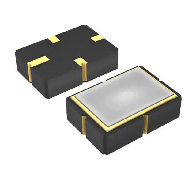
The RO3073A-10 is a true one-port, surface-acoustic-wave (SAW) resonator in a surface-mount, ceramic
case. It provides reliable, fundamental-mode, quartz frequency stabilization of fixed-frequency transmitters
operating at 315.050 MHz. This SAW is designed for remote-control and wireless security transmitters.
Absolute Maximum Ratings
Rating
Value
Units
CW RF Power Dissipation (See: Typical Test Circuit)
+0
dBm
DC Voltage Between Terminals (Observe ESD Precautions)
±30
VDC
-40 to +85
°C
260
°C
Case Temperature
Soldering Temperature (10 seconds / 5 cycles maximum)
Characteristic
Center Frequency (+25 °C)
Absolute Frequency
Tolerance from 315.050 MHz
Insertion Loss
Quality Factor
Temperature Stability
Frequency Aging
Sym
fC
Notes
Minimum
314.975
IL
1.5
Unloaded Q
QU
8000
50 Loaded Q
QL
Turnover Temperature
TO
Turnover Frequency
fO
fC
Frequency Temperature Coefficient
FTC
0.032
Absolute Value during the First Year
|fA|
Maximum
315.125
Units
MHz
±75
kHz
2.2
dB
40
°C
1300
10
25
10
1.0
ppm/°C2
ppm/yr
M
Motional Resistance
RM
19.4
Motional Inductance
LM
78.4
µH
Motional Capacitance
CM
3.3
fF
Shunt Static Capacitance
Test Fixture Shunt Inductance
CO
4.1
pF
LTEST
64.2
nH
Lid Symbolization (in addition to Lot and/or Date Codes)
Standard Reel Quantities
Typical
fC
DC Insulation Resistance between Any Two Terminals
RF Equivalent RLC Model
SM5035-4
782, YYWWS
7/13 inch Reel Sizes
500/3000 pieces/reel
CAUTION: Electrostatic Sensitive Device. Observe precautions for handling.
NOTES:
1. The design, manufacturing process, and specifications of this device are subject to change.
2. US or International patents may apply.
3. RoHS compliant from the first date of manufacture.
© 2004 by RFM Integrated Device Inc.
RO3073A-10 (R) 06/11/2021
Page 1 of 4
www.rfmi.co
�Electrical Connections
Typical Local Oscillator Applications
Terminal
Output
Case Ground
Case Ground
The SAW resonator is bidirectional and may be
installed with either orientation. The two terminals
are interchangeable and unnumbered. The callout
NC indicates no internal connection. The NC pads
assist with mechanical positioning and stability.
External grounding of the NC pads is
recommended to help reduce parasitic
capacitance in the circuit.
+VDC
C1
+VDC
Terminal
L1
C2
RO3XXXA
Bottom View
Typical Test Circuit
The test circuit inductor, LTEST, is tuned to resonate with the static
capacitance, CO, at FC.
RF Bypass
Equivalent LC Model
0.05 pF*
ELECTRICAL TEST
Co = Cp + 0.05 pF
Cp
From 50
Network Analyzer
To 50
Network Analyzer
Rm
Lm
*Case Parasitics
Cm
Temperature Characteristics
POWER TEST
P
INCIDENT
50 Source
P
at F C
REFLECTED
CW RF Power Dissipation =
Low-Loss
Matching
Network to
50
Terminal
NC
NC
Terminal
P INCIDENT - P REFLECTED
Typical Application Circuits
Typical Low-Power Transmitter Application
Typical Circuit Board
Land Pattern
L1
(Antenna)
-50
-100
-100
-150
-150
-200
-80 -60 -40 -20
-200
0 +20 +40 +60 +80
T = T C - T O ( °C )
(4 Places)
Typical Dimension:
0.010 to 0.047 inch
(0.25 to 1.20 mm)
200k
C1
0
-50
The circuit board land pattern shown below is one possible design. The
optimum land pattern is dependent on the circuit board assembly process
which varies by manufacturer. The distance between adjacent land edges
should be at a maximum to minimize parasitic capacitance. Trace lengths
from terminal lands to other components should be short and wide to
minimize parasitic series inductances.
+9VDC
Modulation
Input
fC = f O , T C = T O
0
(f-fo) / fo (ppm)
The curve shown on the right
accounts for resonator
contribution only and does not
include LC component
temperature contributions.
47
C2
RO3XXXA
Bottom View
RF Bypass
470
PCB Footprint
© 2004 by RFM Integrated Device Inc.
RO3073A-10 (R) 06/11/2021
Page 2 of 4
www.rfmi.co
�Case Design
Top View
Side View
B
Bottom View
C
E (3x)
4
F (4x)
A
3
1
2
G (1x)
D
Dimensions
Millimeters
Min
Nom
Inches
Max
Min
Nom
Max
A
4.87
5.00
5.13
0.191
0.196
0.201
B
3.37
3.50
3.63
0.132
0.137
0.142
C
1.45
1.53
1.60
0.057
0.060
0.062
D
1.35
1.43
1.50
0.040
0.057
0.059
E
0.67
0.80
0.93
0.026
0.031
0.036
F
0.37
0.50
0.63
0.014
0.019
0.024
G
1.07
1.20
1.33
0.042
0.047
0.052
© 2004 by RFM Integrated Device Inc.
RO3073A-10 (R) 06/11/2021
Page 3 of 4
www.rfmi.co
�Recommended Reflow Profile
1.
2.
3.
4.
Preheating shall be fixed at 150~180° for 60~90 seconds.
Ascending time to preheating temperature 150° shall be 30 seconds min.
Heating shall be fixed at 220°C for 50~80 seconds and at 260°C peak (10 seconds.)
Time: 5 times maximum
© 2004 by RFM Integrated Device Inc.
RO3073A-10 (R) 06/11/2021
Page 4 of 4
www.rfmi.co
�
很抱歉,暂时无法提供与“RO3073A-10”相匹配的价格&库存,您可以联系我们找货
免费人工找货