QVMQF57425-2.0A-95.573 数据手册
QMQF574T Series
QVMQF574T Series
Temperature Compensated Crystal Oscillators (TCXOs)
TCXOs with Voltage Control Function (VCTCXOs)
MERCURY
Since 1973
QMQF574T and QVMQF574T are QuikXO™ (quick-turn delivery) versions of the
MQF574 (a TCXO) and VMQF574 (a VCTCXO) series, respectively. QuikXO™
products, either standard or custom frequencies are produced and shipped
from California USA in 3 to 5 days and available at Mercury eCommerce.
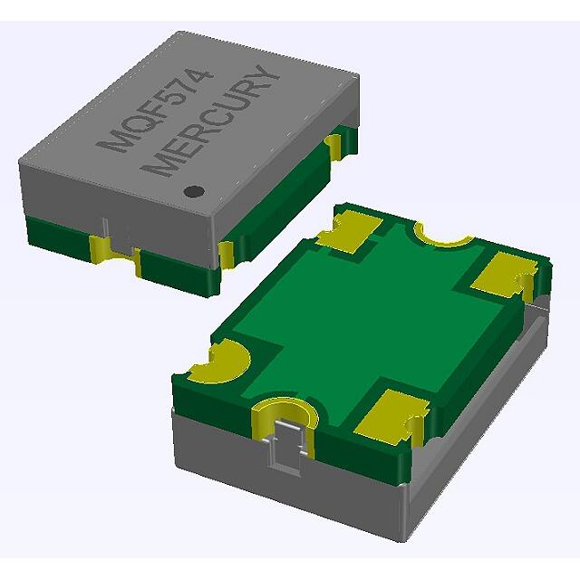
They are 7.0x5.0x2.5 mm SMD, the supply voltage can be either 2.5 V or
3.3 V, CMOS output logics and frequency up to 250 MHz. The 0.8 ~ 1.6 ps
typical phase jitter and lower current consumption (25 mA typical for 250 MHz
at 3.3 V) compared to competitions make the series ideal for multimedia,
Ethernet, and networking applications.
Relevant Categories:
■ For lower cost with regular lead time, please refer to the non- QuikXO™equivalent the MQF574T and
the VMQF574T series
■ For lower phase noise and phase jitter (0.6 p. sec. typical), please refer to MQN574T and VMQN574T series.
■ For smaller footprint, 3.2 x 2.5 x 1.6 mm 6-pad SMD, with the same electrical performance, please refer to the
MQF326T, and the VMQF326T series.
General Specifications: at Ta=+25°C
Output Logic Type
TCXO Models
VCTCXO Models
Frequency Range
Supply Voltage (VDD)
Current Consumption;
typical
Load; typical
Output High Voltage; VOH
Output Low Voltage; VOL
Rise / Fall Time (Tr; Tf)
Frequency Stability vs
CMOS (code “T”)
QMQF574TT25
QVMQF574TT25
10 ~ 250 MHz
+2.5 V ±5%
Code “25”
25 MHz: 17 mA
45 MHz: 20 mA
50 MHz: 21 mA
125 MHz: 24 mA
250 MHz: 25 mA
QMQF574TT33
QVMQF574TT33
10 ~ 250 MHz
+3.3 V ±5%
Code “33”
10 MHz: 21 mA
50 MHz: 24 mA
77 MHz: 25 mA
125 MHz: 29 mA
250 MHz: 34 mA
15 pF
90% VDD min.
10% VDD max.
1.5 nS. Typ.; 3.0 nS. max. (10% ↔ 90% waveform )
±2.0 ppm over -40 to +85°C. Spec. code: “2.0A”.
Operating
±2.5 ppm over -30 to +85°C. Spec. code: “2.5B”.
Temperature
Custom specification: The 2.0A or 2.5B is replaced with a control
number assigned by Mercury.
Voltage Change ±0.2 ppm max. for a ±5% input voltage change
Load Change
MERCURY
±0.2 ppm max. for a ±10% load condition change
www.mercury-crystal.com
Taiwan: TEL (886)-2-2406-2779, e-mail: sales-tw@mercury-crystal.com
U.S.A.: TEL (1)-909-466-0427, e-mail: sales-us@MercuryUnited.com
MERCURY
Page 1 of 5
April 22, 2021
Version: a3
�Aging at
Ta =+25°C
Reflow
Initial Calibration Tolerance
(Initial Frequency Accuracy)
±2 ppm max. first-year; ±10 ppm max. over 10 years
±1.0 ppm max., one reflow and measured 24 hours afterward.
±1.0 ppm typical; ±2.0 ppm. max. at +25°C±2°C.
Duty Cycle
Current with Output
Disabled
Start-up Time
50% ±5%. At 50% VDD.
Output Enable Time
200 ns max.
Output Disable Time
50 ns max.
5 m. sec. max.
Frequency (MHz)
16
25
49.152
50
54
156.250
Supply Voltage
3.3
3.3
3.3
3.3
3.3
3.3
10 Hz
-92
-88
-85
-80
-77
-63
100 Hz
-116
-109
-108
-103
-106
-91
1 kHz
-131
-125
-121
-117
-119
-109
10 kHz
-139
-132
-126
-124
-125
-115
100 kHz
-140
-134
-127
-127
-126
-116
1 MHz
-158
-151
-146
-145
-145
-137
5 MHz
-163
-157
-154
-148
-153
-147
10 MHz
–
–
-157
-150
-157
-150
20 MHz
–
–
-160
-152
-160
-155
0.76
0.9
1.0
1.1
1.1
1.1
Offset
Single Side-band
Phase Noise
(dBc / Hz; typical)
18 mA typical
Integrated Phase Jitter, RMS
12 kHz to 20 MHz; picosecond
Control Voltage Function on Pad 1 (VCTCXOs only)
Control Voltage (Vcontrol)
Frequency Pulling Range
Vcontol center and range: +1.5 V ± 1.0 V. For both 2.5 VDD and 3.3 VDD
High pull: +8 ppm min. for Vcontol from 1.5 V to +2.5V
Low pull: - 8 ppm min. for Vcontol from 0.5 V to +1.5V
Linearity
±5% typical. ±10% max.
Transfer Function
Positive Transfer
Input Impedance
500 KΩ min.
Bandwidth
10 kHz min. Measured at -3 dB.
Output Enable (OE)
Control
Output Enable Time
Tri-State function on Pad 2
70% of VDD (min.) to enable output. CMOS level. Do not leave this pin floating. If no
connection is desired, please contact Mercury.
30% of VDD (max.) to disable the output. Output is high impedance.
200 n. sec. max.
Output Disable Time
50 n. sec. max.
MERCURY
Page 2 of 5
April 22, 2021
Version: a3
�Absolute Maximum Rating:
Input Voltage
Output Voltage
Positive Supply Voltage
-0.5 V to VDD+0.5 V
-0.5 V to VDD+0.5 V
4.2 V
Human Body Model (HBM): Exceeds 2000 V. Class 2 per MIL-STD-1686C
Machine Model (MM): Exceeds 120 V. Class M2 per MIL-STD-1686C.
Note: Power, ground, and outputs are 200 V.
Charged-Device Model (CDM): Exceeds 2000 V. Class C6 per MIL-STD-1686C
Electrostatic Discharge
(ESD)
Environmental Performance Specifications
Moisture Sensitivity Level
RoHS compliant, Pb (lead) free per EU Directive 2002/95/EC
6/6 (2002/95/EC) and WEEE (2002/96/EC). Free of halide, cadmium, hexavalent
chromium, lead, mercury, PBB’s, and PBDE’s.
Level 2 per IPC/JEDEC J-STD-020D.1
Storage temperature range
-55 to +125°C
Humidity
85% RH, 85°C, 48 hours
Fine Leak / Gross Leak
MIL-Std-883, method 1014, condition A / MIL-Std-883, method 1014, condition C
Solderability
MIL-STD-202F method 208E
Reflow
260°C for 10 sec. 2X.
Vibration
MIL-STD-202F method 204, 35G, 50 to 2000 Hz
Shock
MIL-STD-202F method 213B, test condition. E, 1000GG ½ sine wave
Resistance to Solvent
MIL-STD-202, method 215
Temperature Cycling
MIL-STD-883, method 1010
Gold (0.3 um to 1.0 um) over nickel (1.27 um to 8.89 um)
Green Requirement
Pad Surface Finish
Part Number Format and Examples:
Example 1: QVMQF574T33-2.0A-125.000;
Example 3: QMQF574T33-xxxxx-155.520
QVMQF
QMQF
QMQF
574
574
574
Example 2: QMQF574T25-2.5B-148.500;
T
T
T
Product Series
“QMQF”: TCXO
“QVMQF”: VCTCXO
Package Code
“574”:
Output Logic
7.0x5.0x2.5
“T”: CMOS
mm 4-pad SMD
MERCURY
Page 3 of 5
33
25
33
Supply Voltage
“33” for 3.3V
“25” for 2.5V
2.0A
2.5B
xxxxx
-
-
“2.5B”: The freq. stability is
±2.5 ppm over -30 to +85°C
“2.0A”: The freq. stability is
±2.0 ppm over -40 to +85°C
“xxxxx”: Custom frequency
stability. A control number
assigned by Mercury.
April 22, 2021
-
125.000
148.500
155.520
The nominal
Frequency in
MHz. 3 places or
more after the
decimal.
Version: a3
�Output OE Function on pad 2 Note: Do not leave this pad floating. If “no-connection” is desired, please contact Mercury.
VDD
Pad 2
OE Function
VIH
VIL
Enable Time
Disable Time
High Impedance
Phase Noise Plot of QMQF574T33-89.376 MHz, VDD=+3.3V, CMOS
Test Circuits and Output Waveforms
𝑇1
Duty cycle=(𝑇2) ∗ 100%.
Measured at 50% VDD
CMOS
T2
CMOS
T1
VOH
90%VDD
50%VDD
10%VDD
VOL
Tr
MERCURY
Page 4 of 5
April 22, 2021
Tf
Version: a3
�Package Dimensions and Recommended Solder Pad Layout
Pad #
Pad 1
Pad 2
Pad 3
Pad 4
unit: (mm)
Connection
TCXO: No Connection; VCTCXO: Control Voltage Input
Ground
Output: CMOS
Supply Voltage
Recommended Solder Reflow Profile (per IPC/JEDEC J-STD-020D.1)
Tp
Tsmax
Te
m
pe
rat
ur
e
TL
Max. Ramp Up Rate=3°C/s
Max. Ramp Down Rate=6°C/s
tp
Tc-5°C
User Tp≤Tc
tL
Preheat Area
Tc
Tsmin
Tc-5°C
User tp
ts
25
Time 25°C to Peak
Time
Profile Feature
Sn-Pb Eutectic Assembly
Pb-free Assembly
100⁰C
150⁰C
60 to 120 seconds
3⁰C / sec. max.
150⁰C
200⁰C
60 to 180 seconds
3⁰C / sec. max.
Peak package body temperature (Tp)
183⁰C
60 to 150 seconds
235⁰C
217⁰C
60 to 150 seconds
260⁰C
Time (Tp) within 5⁰C of the classification temperature Tc
10 to 30 seconds
20 to 40 seconds
Ramp-down rate (Tp to TL)
6⁰C / second max.
6⁰C / second max.
Time 25⁰C to peak temperature
6 minutes max.
8 minutes max.
Preheat/Soak
- Temperature min. (Ts min.)
- Temperature max. (Ts max.)
- Time (ts) (Ts min. to Ts max.)
Ramp-up rate (TL to Tp)
Liquidous temperature (TL )
Time (tL) maintained above TL
All temperatures refer to the topside of the package, measured on the package body surface.
MERCURY
Page 5 of 5
April 22, 2021
Version: a3
�
QVMQF57425-2.0A-95.573 价格&库存
很抱歉,暂时无法提供与“QVMQF57425-2.0A-95.573”相匹配的价格&库存,您可以联系我们找货
免费人工找货