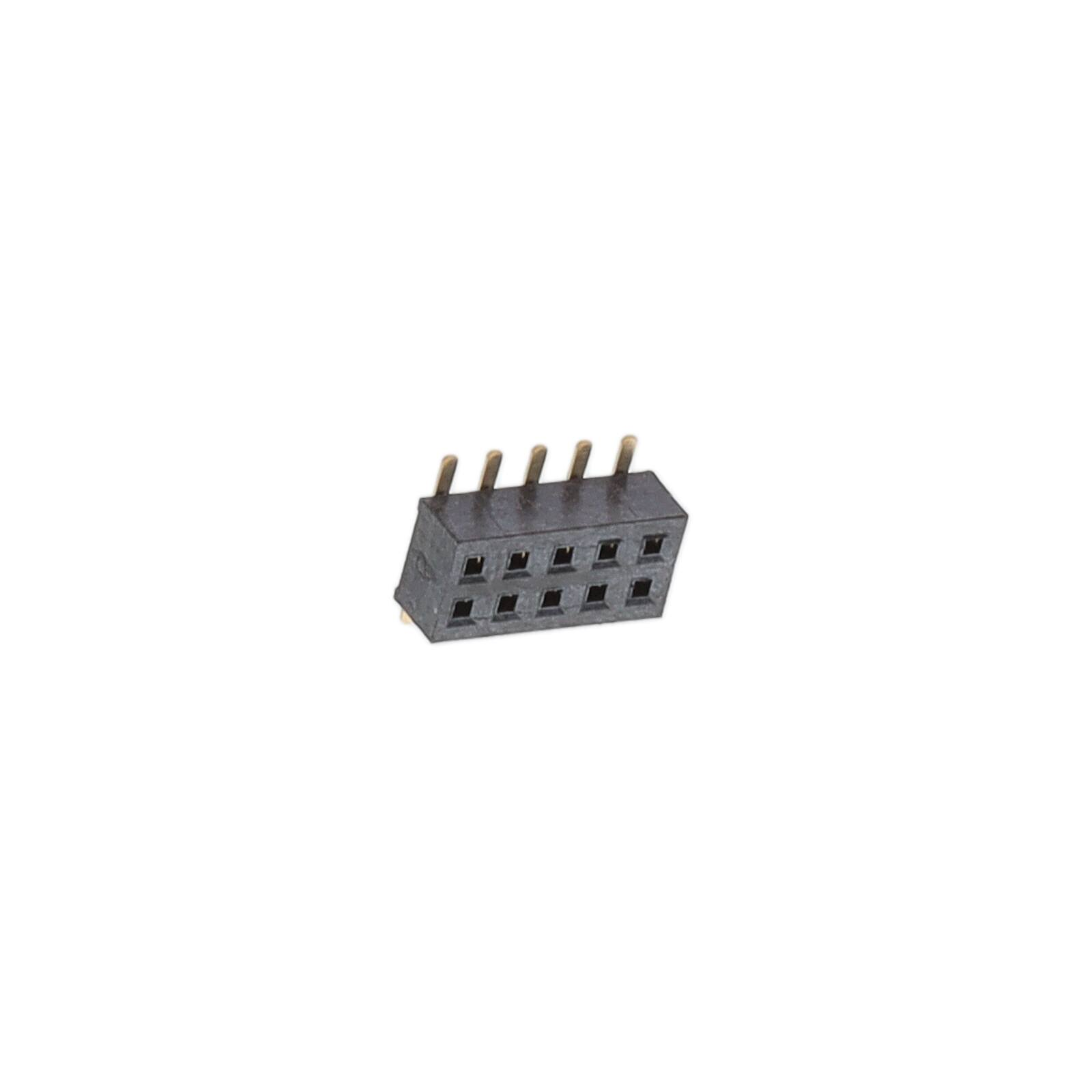
BD050-10-A-0-0500-L-D 数据手册
1.27
1.27
2.00
Ø0.8
0
D +1.0
1.27
2.00
Ø0.8
0
5
Ø0.6
D +1.0
0.42 x 0.15 Pin
H
G
1.27
0.65
A±0.20
B±0.30
0.65
C
C
A
A
For Top Entry
For Bottom Entry
F
Recommended PCB Layouts
C±0.15
0.90
D
Optional Pegs
0.60 Ref.
Ø0.70
2.15
Contact Point
2.00
E
D±0.2
Ordering Grid
Specifications
BD050
B
A
XX
X
X
Locating Peg
0 = Without
1 = With
Mechanical & Environmental
Operating Temperature: -40°C to +105°C
Soldering Process:
IR Reflow: 260°C for 10 sec.
Manual Solder: 350°C for 3-5 sec
Dimension D (1/100mm) (Footprint Width)
0500 = 5.00mm (Standard)
0450 = 4.50mm
Mates with (Subject to pin length)
BD025
BD030
BD035
BD038
BD040
BD095
For bottom entry applications, stringent soldering
control & pin alignment are required as lead to pad
misalignment could cause incorrect mating.
2
3
4
A
B
4
1.27
2.78
/
6
2.54
4.05
1.27
2.54
8
3.81
5.32
5.08
6.59
3.81
12
6.35
7.86
5.08
14
7.62
9.13
6.35
16
8.89
10.40
7.62
18
10.16
11.67
8.89
20
11.43
12.94
10.16
22
12.70
14.21
11.43
24
13.97
15.48
12.70
26
15.24
16.75
13.97
28
16.51
18.02
15.24
30
17.78
19.29
16.51
32
19.05
20.56
17.78
34
20.32
21.83
19.05
36
21.59
23.10
20.32
38
22.86
24.37
21.59
40
24.13
25.64
22.86
42
25.40
26.91
24.13
44
26.67
28.18
25.40
46
27.94
29.45
26.67
48
29.21
30.72
27.94
50
30.48
31.99
29.21
52
31.75
33.26
30.48
54
33.02
34.53
31.75
56
34.29
35.80
33.02
58
35.56
37.07
34.29
60
36.83
38.34
35.56
62
38.10
39.61
36.83
64
39.37
40.88
38.10
66
40.64
42.15
39.37
68
41.91
43.42
40.64
70
43.18
44.69
41.91
72
44.45
45.96
43.18
44.45
74
45.72
47.23
76
46.99
48.50
45.72
78
48.26
49.77
46.99
80
49.53
51.04
48.26
Product Description
BD050
1.27mm Pitch Socket
Dual Row, Surface Mount, Low Profile, Dual Entry
Drawing Date
28th December 2007
By
Revision
Date
5
CC
Tolerances (Except as Noted)
BD050
J PCN
J3
06/03/20
X.° ± 5°
X. ± 0.30
X.X° ± 2°
X.X ± 0.20
X.XX ± 0.15 X.XX° ± 1°
X.XXX ± 0.10 X.XXX° ± 0.5°
Length
Angle
6
Units:
Metric (mm)
C
3rd Angle Projection
7
C
10
Part Number
Detail
1
Request Samples
and Quotation
Packing Options
B = Tape & Reel with Cap (Standard)
C = Tape & Reel with Film
D = Tube
E = Tube with Cap
F = Tube with Film
Insulator Material
L = LCP
Contact Plating
A = Gold Flash All Over (Standard)
C = Tin All Over
Plating
See Ordering Grid
Electrical
Current Rating: 1A per pin
Contact Resistance: 20 mΩ max.
Insulating Resistance: 1000 MΩ min.
Dielectric Withstand Voltage: 500V AC
X
L
XXXX
No. of Contacts
04 to 80
Material
Insulator Material: LCP, UL 94V-0
Contact Terminal: Phosphor Bronze
C
Solder Area
3.00
0.34 Ref.
Dimensions
Number of
Contacts
This drawing is confidential and
copyright of Global Connector
Technology, Ltd (GCT).
This drawing must not be copied
or disclosed without written
consent. E & OE
www.gct.co
Not to
Scale
Drawn By
PKN
8
Sheet No.
1/1
�
BD050-10-A-0-0500-L-D 价格&库存
很抱歉,暂时无法提供与“BD050-10-A-0-0500-L-D”相匹配的价格&库存,您可以联系我们找货
免费人工找货- 国内价格 香港价格
- 1+7.648281+0.95573
- 89+5.5456089+0.69298
- 178+5.28029178+0.65983
- 534+4.88622534+0.61058
- 1068+4.652791068+0.58141
- 5073+4.168465073+0.52089
- 10057+3.9721010057+0.49636
