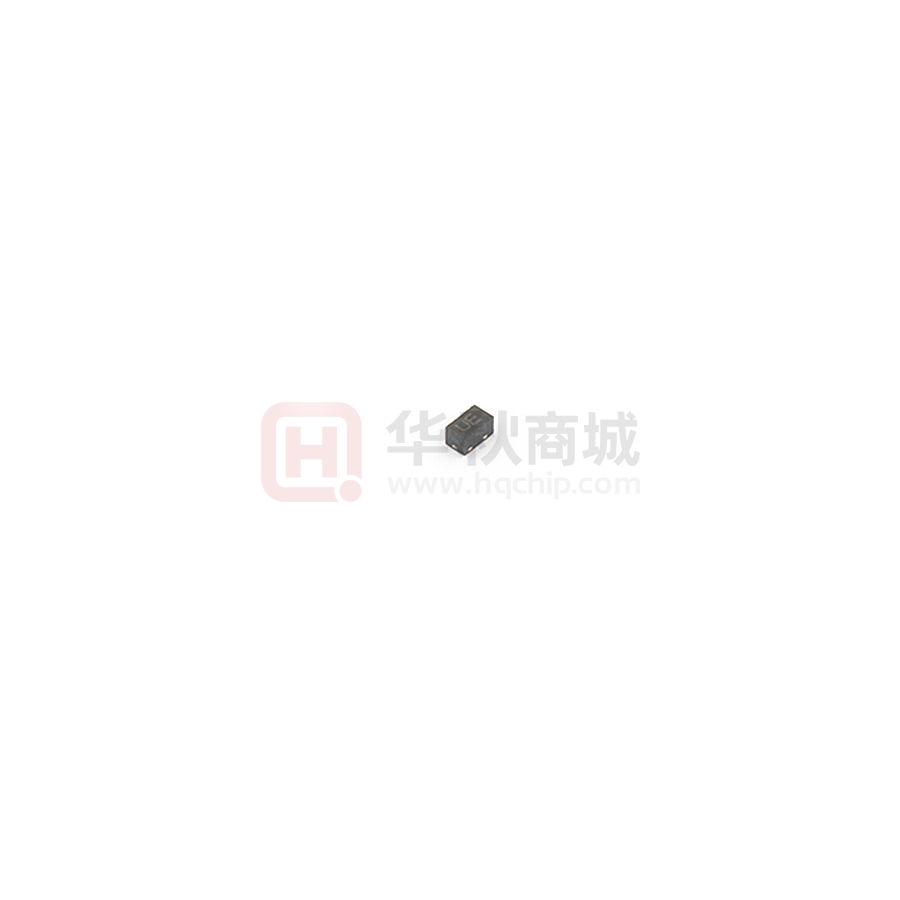
PESD5V0X1BL-N
ESD Protection Diode
»Features
■
120Watts peak pulse power (tp = 8/20μs)
■
Tiny DFN1006 package
■
Bidirectional configurations
■
Solid-state silicon-avalanche technology
■
Low clamping voltage
■
Low leakage current
■
Low capacitance (Cj=0.7pF typ.)
■
Protection one data/power line
■
IEC 61000-4-2 ±30V contact ±30kV air
■
1.2/50μs 12ohm 2kV (GbE PHY side)
■
10/700μs 40ohm 4kV (GbE PHY side )
»Applications
»Mechanical Data
■
10/100/1000Ethernet
■
DFN1006 package
■
Intergated Magnetics/RJ45Connectors
■
Molding compound flammability rating: UL 94V-0
■
LAN/WAN Equipment
■
Packaging: Tape and Reel
■
Notebooks, Desktops, and Servers
■
RoHS/WEEE Compliant
■
Portable Instrumentation
»Schematic & PINConfiguration
DFN1006
Revision 2018
www.born-tw.com
1/5
�PESD5V0X1BL-N
»Absolute MaximumRating
Rating
Symbol
Value
Units
Peak Pulse Power ( tp =8/20μs)
PPP
120
Watts
Peak Pulse Current ( tp =8/20μs)(note1)
Ipp
7
A
VESD
30
30
kV
Lead SolderingTemperature
TL
260(10seconds)
℃
Junction Temperature
TJ
-55 to + 125
℃
Storage Temperature
Tstg
-55 to + 125
℃
ESD per IEC 61000-4-2 (Air)
ESD per IEC 61000-4-2(Contact)
»ElectricalCharacteristics
Parameter
Symbol
Reverse Stand-OffVoltage
Conditions
Min
VRWM
VT
IT=1mA
Reverse LeakageCurrent
IR
VRWM=5V,T=25℃
Peak PulseCurrent
IPP
tp =8/20μs
ClampingVoltage
VC
IPP=7A,tp=8/20μs
JunctionCapacitance
Cj
VR = 0V, f =1MHz
TriggerVoltage
Typical
7.5
Max
Units
5.0
V
8.4
20
V
100
nA
7
A
16
20
V
0.7
0.8
pF
»Electrical Parameters (TA = 25°C unless otherwisenoted)
Symbol
Parameter
I PP
Maximum Reverse Peak Pulse Current
VC
Clamping Voltage @ I PP
V RWM
IR
VT
IT
Working Peak Reverse Voltage
Maximum Reverse Leakage Current @ V RWM
IPP
VTVC
VBR
Trigger Voltage @ I T
VRWM IT
IR
ITIR
VRWM
VBR
VC
VT
Test Current
IPP
Note:. 8/20μs pulsewaveform.
Revision 2018
www.born-tw.com
2/5
�PESD5V0X1BL-N
»Typical Characteristics
Figure 2: Power Derating Curve
10
110
100
1
120w 8/20µs waveform
0.1
1
0.010.1
10
100
90
Percent of Rated Power for Ip p
P p p – Peak Pulse Powe r - Ppp (KW )
Figure 1: Peak Pulse Power vs. Pulse Time
80
70
60
50
40
30
20
10
0
0
1,000
25
td – Pulse Duration -µs
Figure3: Pulse Waveform
Percen t
Ip p
80
e-1
50
40
td=Ipp/2
20
14
12
8
6
4
2
Revision 2018
10
15
Time (µs)
20
25
30
Test
Waveform
Paramters
tr=8µs
td=20µs
10
0
5
150
16
10
0
125
18
Clamping Voltage–V C (V)
90
30
100
20
W aveform
Paramters
tr=8µs
td=20µs
100
60
75
Figure 4: Clamping Voltage vs.Ipp
110
70
50
Ambient Temperature - TA (℃)
0
2
4
6
8
10
12
Peak Pulse Current–IPP (A)
www.born-tw.com
3/5
�PESD5V0X1BL-N
»Lightning Surge Test Results for Gigabit Ethernet
During the metallic (line-to-line) surge test, the line being stressed is tied to the surge generator with the remaining lines
tied together and connected to the generator ground. Current will flow through the line transformer transferring energy to
the PHY side of the transformer. Figure 5 shows the test set-up for measuring the clamping voltage of the device.This set up
is designed to test the surge in an actual gigabit Ethernet (GbE) circuit. Two 4.7 Ohm resistors is usedfor decoupling. The
clamping voltage of the PESD5V0X1BL-N for a metallic mode 4000V (10/ 700μs) surge.The clamping voltage, measured at
less than 13 volts, provides sufficient clamping margin to minimize electrical stress and is well below the failure voltage
range of typical GbE PHY chips .
Ipp
R L =4.7 Ω
+
+
Vin
Vc
R L =4.7 Ω
-
Gigabit
Ethernet
Phy
-
Figure5-Clamping VoltageTestSet-Up
RJ-45
PESD5V0X1BL-N
Gigabit
Ethernet
PHY
PESD5V0X1BL-N
Figure 6 - GbE Protection to Lightning, ESD, and CDE
Revision 2018
www.born-tw.com
4/5
�PESD5V0X1BL-N
»Outline Drawing –DFN1006
Marking
UE
Ordering information
Ordercode
PESD5V0X1BL-N
Revision 2018
Package
DFN1006
Base qty
10k
www.born-tw.com
Deliverymode
Tape andreel
5/5
�
很抱歉,暂时无法提供与“PESD5V0X1BL-N”相匹配的价格&库存,您可以联系我们找货
免费人工找货- 国内价格
- 20+0.23912
- 200+0.19188
- 600+0.16563
- 2000+0.14989
- 10000+0.11937
- 20000+0.11198
- 国内价格
- 1+0.22990
- 500+0.15290
- 5000+0.13310
- 10000+0.12100
- 国内价格
- 10+0.23359
- 100+0.18809
- 2000+0.14824
- 4000+0.11628
