SDA33W5

SDA33W5

  • 厂商:

    LEIDITECH(雷卯电子)

  • 封装:

    SOT-353-5(SC-70-5)

  • 描述:

    ESD保护 VRWM=3 V VBR(Min)=4.5 V VC=15.3 V IPP=4 A Ppp=100 W SOT353

  • 详情介绍
  • 数据手册
  • 价格&库存
SDA33W5 数据手册
SDA33W5 BI-DIRECTIONAL TVS DIODE ARRAY FOR ESD AND LATCH-UP PROTECTION Features  Low leakage current  Operating voltage: 3.3V  Low clamping voltage  JEDEC SOT-353 package  Complies with following standards: – IEC 61000-4-2 (ESD) immunity test Air discharge: ±30kV Contact discharge: ±30kV – IEC61000-4-5 (Lightning) 8A (8/20μs)  RoHS Compliant Dimensions SOT-353 Applications  Peripherals  Industrial Equipment  Notebook Computers  Portable Instrumentation  Microprocessor Based Equipment  Cell Phone Handsets and Accessories  Personal Digital Assistants (PDAs) and Pagers Pin Configuration Mechanical Characteristics  Package: SOT-353  Lead Finish: Matte Tin  Case Material: “Green” Molding Compound.  Moisture Sensitivity: Level 3 per J-STD-020  Terminal Connections: See Diagram Below  Marking Information: See Below Absolute Maximum Ratings(Tamb=25°C unless otherwise specified) Parameter Peak Pulse Power (8/20µs) ESD per IEC 61000−4−2 (Air) Symbol Ppp Value Unit 100 W ±30 VESD Kv ±30 ESD per IEC 61000−4−2 (Contact) Operating Temperature Range TJ -55 to +125 ℃ Storage Temperature Range TSTJ -55 to +150 ℃ Rev : 01.06.2017 1/4 www.leiditech.com SDA33W5 Electrical Characteristics(TA=25°C unless otherwise specified) Vc Part Number SDA33W5 Rev : 01.06.2017 Device Marking VRWM (V) VBR (V) IT (mA) VC @1A F05 3.3 4.5 1 8 2/4 (Max) 12 (@A) 8 IR μA (Max) C (Pf) (Typ.) 0.2 60 www.leiditech.com SDA33W5 Typical Performance Characteristics (TA=25°C unless otherwise Specified) Junction Capacitance vs. Reverse Voltage Peak Pulse Power vs. Pulse Time Clamping Voltage vs. Peak Pulse Current Power Derating Curve Note:Data is taken with a 10x attenuator ESD Clamping Voltage 8 X 20μs Pulse Waveform Rev : 01.06.2017 8 kV Contact per IEC61000−4−2 3/4 www.leiditech.com SDA33W5 SOT-353 Package Outline & Dimensions Inches Symbol Min. A 0.031 0.037 0.043 0.80 0.95 1.10 A1 0.000 0.002 0.004 0.00 0.05 0.10 A3 0.08 REF 0.2 REF b 0.004 0.008 0.012 0.10 0.21 0.30 C 0.004 0.005 0.010 0.10 0.14 0.25 D 0.070 0.078 0.086 1.80 2.00 2.20 E 0.045 0.049 0.053 1.15 1.25 1.35 e Soldering Footprint Millimeters Nom. Max. Min. Nom. Max. 0.026 BSC 0.65 BSC L 0.004 0.008 0.012 0.10 0.20 0.30 HE 0.078 0.082 0.086 2.00 2.10 2.20 Symbol Inches Millimeters C 0.0748 1.9 G 0.055 1.40 P 0.025 0.65 P1 0.051 1.30 X 0.0157 0.40 Y 0.019 0.50 Z 0.0945 2.4 Shanghai Leiditech Electronic Co.,Ltd Email: sale1@leiditech.com Tel : +86- 021 50828806 Fax : +86- 021 50477059 Rev : 01.06.2017 4/4 www.leiditech.com
SDA33W5
物料型号:SDA33W5

器件简介:该器件具有低漏电流、低钳位电压,符合JEDEC SOT-353封装标准,并通过IEC 61000-4-2(ESD)和IEC61000-4-5(闪电)标准测试。

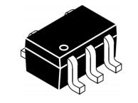
引脚分配:文档中提供了SOT-353封装的引脚配置图,但未提供具体的引脚分配信息。

参数特性:包括工作电压3.3V、最大钳位电压4.5V、漏电流1mA、在1A电流下的电压降8V、最大反向电压12V、最大反向电流0.2μA、电容60pF。

功能详解:文档描述了器件的典型性能特性,如峰值脉冲功率与脉冲时间的关系、钳位电压与峰值脉冲电流的关系以及功率降额曲线。

应用信息:适用于外围设备、工业设备、笔记本电脑、便携式仪器、基于微处理器的设备、手机及其配件、个人数字助理(PDA)和寻呼机。

封装信息:SOT-353封装,引脚镀锡,采用“绿色”模具化合物,湿度敏感等级为3级,符合J-STD-020标准。