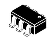
SRV05-4W
LOW CAPACITANCE TVS DIODE ARRAY
Features
●
●
●
●
●
●
Ultra low leakage: nA level
Operating voltage: 5V
Low clamping voltage
Complies with following standards:
– IEC 61000-4-2 (ESD) immunity test
Air discharge: ±30kV
Contact discharge: ±30kV
– IEC61000-4-4 (EFT) 40A (5/50ns)
– IEC61000-4-5 (Lightning) 25A (8/20μs)
RoHS Compliant
Dimensions SOT-26
AEC -Q101 qualified.
Pin Configuration
Applications
●
●
●
●
●
●
USB 2.0 power and data line
Set-top box and digital TV
Digital video interface (DVI)
Notebook Computers
SIM Ports
10/100/1000 Ethernet
Mechanical Characteristics
●
Package: SOT-26
●
Lead Finish: Lead Free
●
UL Flammability Classification Rating 94V-0
●
Quantity Per Reel:3,000pcs
●
Reel Size:7inch
●
Device Marking: SRV05
Absolute Maximum Ratings(Tamb=25°C unless otherwise specified)
Parameter
Peak Pulse Power (8/20µs)
ESD per IEC 61000−4−2 (Air)
Symbol
Ppp
Value
Unit
500
W
±30
VESD
Kv
±30
ESD per IEC 61000−4−2 (Contact)
Operating Temperature Range
TJ
-55 to +125
℃
Storage Temperature Range
TSTJ
-55 to +150
℃
Rev : 01.06.2018
1/8
www.leiditech.com
�SRV05-4W
Electrical Characteristics(TA=25°C unless otherwise specified)
Parameter
Reverse Working Voltage
Breakdown Voltage
Symbol
Min
Typ
VRWM
VBR
Max
Unit
5
V
6
Test Condition
V
IT = 1mA, Pin 5 to Pin 2
Reverse Leakage Current
IR
1
µA
VRWM = 5V, Pin 5 to Pin 2
Forward Voltage
VF
1.2
V
IF = 15mA
Clamping Voltage
VC
12
V
IPP = 1A (8 x 20µs pulse), any I/O
pin to ground
Clamping Voltage
VC
20
V
IPP = 25A (8 x 20µs pulse), any I/
O pin to ground
Junction Capacitance
CJ
1.5
pF
VR = 0V, f = 1MHz, between I/O
pins
Junction Capacitance
CJ
3.0
pF
VR = 0V, f = 1MHz, any I/O pin to
ground
5.0
Note 1: I/O pins are Pin 1, 3, 4 and 6
Rev : 01.06.2018
2/8
www.leiditech.com
�SRV05-4W
Typical Performance Characteristics (TA=25°C unless otherwise Specified)
Junction Capacitance_Cj (pF)
5
4
Line to GND
3
2
Line to Line
1
0
0
1
2
3
4
Reverse Voltage_VR (V)
5
Junction Capacitance vs. Reverse Voltage
Peak Pulse Power vs. Pulse Time
120
% of Rated Power
100
80
60
40
20
0
0
25
50
75
100 125
Ambient Temperature_Ta(℃)
150
Power Derating Curve
Clamping Voltage vs. Peak Pulse Current
100
% of Peak Pulse Current
90
80
70
60
50
40
30
20
10
0
0
20
40
Time_t(uS)
60
80
Note:Data is taken with a 10x attenuator
ESD Clamping Voltage
8 X 20μs Pulse Waveform
8 kV Contact per IEC61000−4−2
Rev : 01.06.2018
3/8
www.leiditech.com
�SRV05-4W
Typical Application
The SRV05-4W is designed to protect four data lines from transient over
-voltages by clamping them to fixed reference.
When the voltage on the protected line exceeds the reference voltage (plus diode VF) the steering diodes are for
ward biased, conducting the transient current away from the sensitive circuitry. Data lines are connected at pins 1, 3,
4 and 6. The negative reference (REF1) is connected at pin 2. This pin should be connected directly to a ground
plane on the board for best results. The path length is kept as short as possible to minimize parasitic inductance.
The positive reference (REF2) is connected at pin 5.
I/O 1
To Protected IC
I/O 2
6
1
2
5
3
4
VCC
I/O 3
I/O 4
To Protected IC
SRV05-4W on Video Interface Application
VCC
6
5
4
1
2
3
VCC
6
1
Rev : 01.06.2018
5
2
4
3
4/8
www.leiditech.com
�SRV05-4W
SRV05-4W on USB Port Application
Vbus
D+
D-
USB Port
Vbus
6
5
4
1
2
3
GND
USB
Controller
Vbus
D+
D-
USB Port
GND
SRV05-4W on SIM Port Application
I/O
Clock
Reset
SIM
Vcc
GND
Rev : 01.06.2018
6
5
4
1
2
3
5/8
www.leiditech.com
�SRV05-4W
SRV05-4W on Digital Visual Interface (DVI) Application
PC Graphics Card
Flat Panel Display
5
2
3
4
3
1
6
2
6
1
5
RX0RX0+
4
TX0TX0+
5
2
3
4
3
LCD
1
6
2
6
1
5
RX1RX1+
RX2RX2+
4
TX1TX1+
TX2TX2+
VGA
TCTC+
RCRC+
DM Transmitter
TMDS Receiver
SRV05-4W on Ethernet 10/100 (Differential mode) Application
TX+
TX+
TX-
TXRX+
RJ45
Connector
Coupling
Transformer
RX+
RX-
RX1
6
2
5
3
4
VCC
GND
Rev : 01.06.2018
6/8
www.leiditech.com
�SRV05-4W
SRV05-4W on T1/E1 Interface Application
R1
RTIP
RRING
VCC
T1
R2
6
5
4
1
2
3
T1/E1
Tranceiver
R3
TTIP
TRING
Rev : 01.06.2018
T2
R4
7/8
www.leiditech.com
�SRV05-4W
SOT-26 Package Outline & Dimensions
Inches
Symbol
Min.
A
θ
Nom. Max. Min. Nom. Max.
0.035
-
0.057 0.90
-
1.45
A1
0.000
-
0.006 0.00
-
0.15
A2
0.035 0.045 0.051 0.90 1.15 1.30
b
0.010
-
0.020 0.25
-
0.50
-
0.009 0.08
-
0.22
c
0.003
D
0.110 0.114 0.122 2.80 2.90 3.10
E1
0.060 0.063 0.069 1.50 1.60 1.75
E
0.110 BSC
2.80 BSC
e
0.037 BSC
0.95 BSC
e1
0.075 BSC
1.90 BSC
L
0.012 0.018 0.024 0.30 0.45 0.60
L1
θ
Soldering Footprint
Millimeters
(0.024)
0°
-
(0.60)
10°
0°
-
10°
aaa
0.004
0.10
bbb
0.008
0.20
ccc
0.008
0.20
Symbol
Inches
Millimeters
C
(0.098)
(2.50)
G
0.055
1.40
P
0.037
0.95
X
0.024
0.60
Y
0.043
1.10
Z
0.141
3.60
Shanghai Leiditech Electronic Co.,Ltd
Email: sale1@leiditech.com
Tel : +86- 021 50828806
Fax : +86- 021 50477059
Rev : 01.06.2018
8/8
www.leiditech.com
�
很抱歉,暂时无法提供与“SRV05-4W”相匹配的价格&库存,您可以联系我们找货
免费人工找货