ULC052510BP10
ULTRA LOW CAPACITANCE TVS DIODE ARRAY
Features
●
●
●
●
●
Ultra low leakage: nA level
Operating voltage: 5V
Low clamping voltage
Complies with following standards:
– IEC 61000-4-2 (ESD) immunity test
Air discharge: ±17kV
Contact discharge: ±15kV
– IEC61000-4-4 (EFT) 40A (5/50ns)
– IEC61000-4-5 (Lightning) 2.5A (8/20μs)
RoHS Compliant
Dimensions DFN2510P10
Applications
●
●
●
●
●
●
●
Pin Configuration
USB 2.0/3.1 power and data line
Set-top box and digital TV
Digital video interface (DVI)
Notebook Computers
SIM Ports
10/100/1000 Ethernet
HDMI 2.0
Mechanical Characteristics
●
Package: DFN2510P10
●
Lead Finish: Lead Free
●
UL Flammability Classification Rating 94V-0
●
Quantity Per Reel:3,000pcs
●
Reel Size:7 inch
Absolute Maximum Ratings(Tamb=25°C unless otherwise specified)
Parameter
Peak Pulse Power (8/20µs)
ESD per IEC 61000−4−2 (Air)
Symbol
Ppp
VESD
Value
50
±17
Unit
W
Kv
±15
ESD per IEC 61000−4−2 (Contact)
Operating Temperature Range
TJ
-55 to +125
℃
Storage Temperature Range
TSTJ
-55 to +150
℃
Rev : 01.06.2014
1/ 7
www.leiditech.com
�ULC052510BP10
Electrical Characteristics(TA=25°C unless otherwise specified)
Vc
Part Number
ULC052510BP10
Device
Marking
VRWM
(V)
VBR
(V)
IT
(Ma)
VC
@1A
UL14
5
6
1
18
(Max)
30
(@A)
2.5
IR
Μa
(Max)
C
(Pf)
(Typ.)
1
0.2
Characteristic Curves
Fig2. ESD Pulse Waveform (according to IEC 61000-4-2)
Fig1. 8/20µ s Pulse Waveform
120
IPP - Peak Pulse Current - % of IPP
100
100%
TEST
WAVEFORM
PARAMETERS
tr=8 s
td=20 s
Peak Value IPP
80
Percent of Peak Pulse Current %
tr
60
40
td=t IPP/2
20
0
0
5
10
15
20
25
10%
tr = 0.7~1ns
Time (ns)
30ns
30
60ns
t - Time ( s)
Fig3.
90%
Power Derating Curve
% of Rated Power
110
100
90
80
70
60
50
40
30
20
10
0
0
25
50
75
100
125
150
Ambient Temperature –TA (ºC)
Rev : 01.06.2014
2/7
www.leiditech.com
�ULC052510BP10
Transmission Line Pulse (TLP)
Transmission Line Pulse (TLP) is a measurement technique used in the Electrostatic Discharge (ESD) arena
to characterize performance attributes of devices under ESD stresses. TLP is able to obtain current versus
voltage (I−V) curves in which each data point is obtained with a 100 ns long pulse, with currents up to 40 A.
TLP was first used in the ESD field to study human body model (HBM) in integrated circuits, but it is an
equally valid tool in the field of system level ESD. The applicability of TLP to system level ESD is illustrated
in Figure 1, which compares an 8 kV IEC 61000−4−2 current waveform with TLP current pulses of 8 and 16 A.
The current levels and time duration for the pulses are similar and the initial rise time for the TLP pulse is
comparable to the rise time of the IEC 61000−4−2’s initial current spike. This application note will give a
basic introduction to TLP measurements and explain the datasheet parameters extracted from TLP for
Yeashin Technology’s protection products.
Comparison of a Current
Waveform of IEC 61000−4−2
with TLP Pulses at 8 and 16 A.
The IEC 61000−4−2 ESD
waveforms is true to the
Standard and is shown here
as captured on an oscilloscope.
The points A, B, and C show
the points on the waveforms
specified in IEC 61000−4−2.
TLP Characteristic (Positive)
Rev : 01.06.2014
TLP Characteristic (Negetive)
3/ 7
www.leiditech.com
�ULC052510BP10
Eye Diagram
1
2
3
4
5
6
7
8
9
Rev : 01.06.2014
Zero Level : measure of the mean value of the logical 0.
One Level : measure of the mean value of the logical 1.
Rise Time : measure of the transition time of the
data from the 10% level to the 90% level on the
upward slope.
Fall Time : measure of the transition time of the
data from the 90% level to the 10% level on the
downward slope.
Eye Height : measure of the vertical opening.
Determine eye closure due to noise.
Eye Width : measure of the horizontal opening.
Determine influence of jitter on the eye opening.
Deterministic Jitter : deviation of a transition
from its ideal time caused by reflections relative
to other transitions.
Eye Amplitude : difference between the logic 0
level and the logic 1 level histogram mean value.
Bit Rate : inverse of the bit period.
4/ 7
www.leiditech.com
�ULC052510BP10
Eye Diagram at 5Gbps and 10Gbps
Rev : 01.06.2014
5/ 7
www.leiditech.com
�ULC052510BP10
LAYOUT DIAGRAM INFORMATION
Figure 1. USB 3.1 Layout Diagram
Figure 2. HDMI 2.0 Layout Diagram
Rev : 01.06.2014
6/ 7
www.leiditech.com
�ULC052510BP10
DFN2510P10 PACKAGE OUTLINE & DIMENSIONS
* SOLDERING FOOTPRINT
Shanghai Leiditech Electronic Co.,Ltd
Email: sale1@leiditech.com
Tel : +86- 021 50828806
Fax : +86- 021 50477059
Rev : 01.06.2014
7/7
www.leiditech.com
�
很抱歉,暂时无法提供与“ULC052510BP10”相匹配的价格&库存,您可以联系我们找货
免费人工找货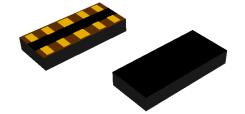


 工商网监
湘ICP备2023018690号
工商网监
湘ICP备2023018690号