ULC3304P10
Ultra Low Capacitance TVS Diode Array
Features
●
●
●
●
●
●
●
Ultra low capacitance: 0.4pF typical (I/O to I/O)
Ultra low leakage: nA level
Low operating voltage: 3.3V
Low clamping voltage with snap back technology
Up to 4 lines protects
Leadless flow -through package
Complies with following standards:
Dimensions DFN2510P10
– IEC 61000-4-2 (ESD) immunity test
Air discharge: ±30kV
Contact discharge: ±30 kV
●
– IEC61000-4-4 (EFT) 40A (5/50ns)
– IEC61000-4-5 (Lightning) 5A (8/20µs)
RoHS Compliant
Pin Configuration
Applications
●
HDMI 1.3 & 1.4, USB 2.0 & 3.0 and MDDI ports
●
Monitors and flat panel displays
●
Set - top box and Digital TV
●
Video graphics cards
●
Digital Video Interface (DVI)
●
Notebook Computers
●
PCI Express and Serial SATA Ports
Mechanical Characteristics
●
Package: DFN2510P10
●
Lead Finish: Matte Tin
●
UL Flammability Classification Rating 94V-0
●
Quantity Per Reel:3000pcs
●
Reel Size:7inch
●
Device Marking:3324
Absolute Maximum Ratings(Tamb=25°C unless otherwise specified)
Parameter
Peak Pulse Power (8/20µs)
ESD per IEC 61000−4−2 (Air)
Symbol
Ppp
Value
60
Unit
W
±30
VESD
Kv
±30
ESD per IEC 61000−4−2 (Contact)
Operating Temperature Range
TJ
-55 to +125
℃
Storage Temperature Range
TSTJ
-55 to +150
℃
Rev : 01.07.2021
1/9
www.leiditech.com
�ULC3304P10
Electrical Characteristics(TA=25°C unless otherwise specified)
Parameter
Symbol
Reverse Working Voltage
Breakdown Voltage
Min
Typ
VRWM
VBR
Max
Unit
3.3
V
Any I/O pin to ground
V
IT = 1mA, any I/O pin to ground
4.5
Test Condition
Reverse Leakage Current
IR
0.5
µA
VRWM = 3.3V,any I/O pin to ground
Clamping Voltage
VC
3.5
V
IPP = 1A (8 x 20µs pulse), any I/O
pin to ground
Clamping Voltage
VC
12
V
IPP = 5A (8 x 20µs pulse), any I/O
pin to ground
Junction Capacitance
CJ
0.4
pF
VR = 0V, f = 1MHz, between I/O
pins
Junction Capacitance
CJ
0.6
pF
VR = 0V, f = 1MHz, any I/O pin to
ground
Characteristic Curves
10
Peak Pulse Power_Ppp (W)
Junction Capacitance_Cj (pF)
1
0.8
0.6
0.4
0.2
0
1
0.1
0.01
0
1
2
3
4
Reverse Voltage_VR (V)
0.1
5
120
8.00
100
% of Rated Power
Clamping Voltage_Vc (V)
10.00
4.00
2.00
10
100
1000
Pulse Duration_tp (us)
Peak Pulse Power vs. Pulse Time
Junction Capacitance vs. Reverse Voltage
6.00
1
80
60
40
20
0.00
0
1
2
3
4
5
Peak Pulse Current_Ipp (A)
Rev : 01.07.2021
01.06.2014
0
6
0
2/9
2/3
25
50
75
100
125
℃
150
www.leiditech.com
�ULC3304P10
Clamping Voltage vs. Peak Pulse Current
Power Derating Curve
100
% of Peak Pulse Current
90
80
70
60
50
40
30
20
10
0
0
20
40
Time_t(uS)
60
80
ESD Clamping Voltage
8 X 20uS Pulse Waveform
8 kV Contact per IEC61000−4−2
Typical Application
The ULC3304P10 is designed for easy PCB layout by owing
all
the traces to run straight through the device. The PCB
traces could be used to connect the pin pairs for each line. For example, line 1 enters at pin 1 and exits at pin 10 and
the PCB trace connects Pin 1 and Pin 10 together. Ground is connected at Pin 3 and Pin 8.
10
1
9
2
8
3
7
4
6
5
Rev : 01.07.2021
3/9
www.leiditech.com
�ULC3304P10
ULC3304P10 on USB 3.0 Port Application
Vbus
Vbus
DD+
ID
GND
MicB_SSTX-
MicB_SSTX+
GND_DRAIN
MicB_SSRX-
MicB_SSRX+
Rev : 01.07.2021
4/9
www.leiditech.com
�ULC3304P10
ULC3304P10 on DVI Port Application
Rev : 01.07.2021
5/9
www.leiditech.com
�ULC3304P10
ULC3304P10 on HDMI Port Application
TMDS D2+
GND
TMDS D2TMDS D1+
GND
TMDS D1TMDS D0+
GND
TMDS D0HDMI Graphic Video
Controller
TMDS Clock+
GND
TMDS ClockCEC
NC
SCL
SDA
GND
5V Power
Hot Plug Detect
Rev : 01.07.2021
6/9
www.leiditech.com
�ULC3304P10
ULC3304P10 on MDDI Port Application
ULC3304P10
ULC3304P10
ULC0511CDN
ULC0511CDN
ULC0511CDN
ULC0511CDN
ULC3304P10 on 10/100 Base Ethernet Port Application
Rev : 01.07.2021
7/9
www.leiditech.com
�ULC3304P10
ULC3304P10 on VGA Port Application
ULC3304P10 on eSATA Port Application
Rev : 01.07.2021
8/9
www.leiditech.com
�ULC3304P10
DFN2510P10 PACKAGE OUTLINE & DIMENSIONS
* SOLDERING FOOTPRINT
Shanghai Leiditech Electronic Co.,Ltd
Email: sale1@leiditech.com
Tel : +86- 021 50828806
Fax : +86- 021 50477059
Rev : 01.07.2021
9/9
www.leiditech.com
�
很抱歉,暂时无法提供与“ULC3304P10”相匹配的价格&库存,您可以联系我们找货
免费人工找货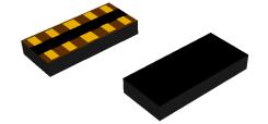


 工商网监
湘ICP备2023018690号
工商网监
湘ICP备2023018690号