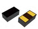
PESD1563U250
1. Electrical Specification
1-1 Test condition
Varistor voltage
Leakage current
Maximum clamping voltage
In = 1 mA DC
Vdc = 15 V DC
Ic = 1 A
Rated peak single pulse transient current
8 / 20 ㎲ waveform, +/- each 1 time induce
Capacitance
10/1000 ㎲ waveform
Insulation resistance after reflow soldering
f = 1MHz, Vrms = 0.5 V
Soldering paste : Tamura (Japan) RMA-20-21L
Stencil : SUS, 120 ㎛ thickness
Reflow soldering condition
Pad size : 0.8 (Width) x 0.9 (Length)
0.8 (Distance between pads)
Soldering profile : 260±5 ℃, 5 sec.
1-2 Electrical specification
Maximum allowable continuous DC voltage
15
V
110-125
V
Maximum clamping voltage
200
V
Maximum
Rated peak single pulse transient current
1
A
Maximum
trigger voltage / Varistor voltage / breakdown voltage
Nonlinearity coefficient
> 12
Leakage current at continuous DC voltage
< 0.1
㎂
Response time
< 0.5
ns
Varistor voltage temperature coefficient
< 0.05
Capacitance measured at 1MHz
Capacitance tolerance
%/℃
2.5
pF
±30
%
Insulation resistance after reflow soldering on PCB
> 10
Operating ambient temperature
-55 to +125
℃
Storage temperature
-55 to +125
℃
Rev : 01.06.2018
1/5
Typical
MΩ
www.leiditech.com
�PESD1563U250
1-3 Reliability testing procedures
Reliability
parameter
Pulse current
capability
Electrostatic
discharge
capability
Test
Imax
8/20 ㎲
ESD
C=150 pF,
R=330Ω
Environmenta
l reliability
Thermal shock
Test methods and remarks
Test requirement
IEC 1051-1, Test 4.5.
dVn/Vn≤ 10%
10 pulses in the same direction at 2
pulses per minute at maximum peak
current
no visible damage
IEC 1000-4-2
dVn/Vn≤ 10%
Each 10 times in positive/negative
direction in 10 sec at 8KV contact
discharge (Level 4)
no visible damage
IEC 68-2-14
dVn/Vn≤ 5%
Condition for 1 cycle
Step 1 : Min. –40℃, 30±3 min.
no visible damage
Step 2 : Max. +125℃, 30±3 min.
Number of cycles: 30 times
Low temperature
IEC 68-2-1
dVn/Vn≤ 5%
Place the chip at -40±5℃ for 1000±
no visible damage
12hrs. Remove and place for 24±2hrs at
room temp. condition, then measure
High temperature
IEC 68-2-2
dVn/Vn≤ 5%
Place the chip at 125±5℃ for 1000±
no visible damage
24hrs. Remove and place for 24±2hrs at
room temp. condition, then measure
Heat resistance
IEC 68-2-3
dVn/Vn≤ 5%
Apply the rated voltage for 1000±48hrs at
no visible damage
85±3℃. Remove and place for 24±2hrs
at room temp. condition, then measure
Humidity
resistance
IEC 68-2-30
dVn/Vn≤ 10%
Place the chip at 40±2℃ and 90 to 95%
no visible damage
humidity for 1000±24hrs. Remove and
place for 24±2hrs at
condition, then measure
Pressure cooker
test
Rev : 01.06.2018
room
temp.
Place the chip at 2 atm, 120℃, 85%RH
dVn/Vn≤ 10%
for 60 hrs. Remove and place for 24±
2hrs at room temp. condition, then
measure
no visible damage
2/5
www.leiditech.com
�PESD1563U250
Operating life
Mechanical
Solderability
Apply the rated voltage for 1000±48hrs at
dVn/Vn≤ 10%
125±3℃. Remove and place for 24±2hrs
at room temp. condition, then measure
no visible damage
IEC 68-2-58
At least 95% of terminal
electrode is covered by
new solder
Solder bath method, 230±5℃, 2s
Reliability
Resistance to
soldering heat
Bending strength
IEC 68-2-58
dVn/Vn≤ 5%
Solder bath method,
260±5℃, 10±0.5s, 270±5℃, 3±0.5s
IEC 68-2-21
dVn/Vn≤ 5%
Warp:2mm, Speed:0.5mm/sec, Duration:
10sec. The measurement shall be made
with board in the bent position
Adhesive strength
no visible damage
IEC 68-2-22
no visible damage
Strength>10 N
Applied force on SMD chip by fracture
from PCB
no visible damage
2. Material Specification
Body
ZnO based ceramics
Internal electrode
Silver – Palladium
External electrode
Silver – Nickel – Tin
Thickness of Ni/Sn plating layer
Nickel > 1 ㎛, Tin > 2 ㎛
3. Dimension Specification
L
T
W
Size
L(mm)
W(mm)
T(mm)
M(mm)
0402
1.0±0.10
0.5±0.10
≤ 0.6
0.20±0.10
0603
1.6±0.15
0.8±0.15
≤ 0.9
0.35±0.10
M
Rev : 01.06.2018
3/5
www.leiditech.com
�PESD1563U250
4. Soldering Recommendations
4-1 Soldering profile
4-1-1 Pb free solder paste
4-1-2 Repair soldering
-
Allowable time and temperature for making correction with a soldering iron
: 350 ± 10 ℃, 3 sec.
-
Optimum solder amount when corrections are made using a soldering iron
4-2 Soldering guidelines
-
Our chip varistors are designed for reflow soldering only. Do not use flow soldering
-
Use non-activated flux (Cl content 0.2% max.)
-
Follow the recommended soldering conditions to avoid varistor damage.
Rev : 01.06.2018
4/5
www.leiditech.com
�PESD1563U250
4-3 Solder pad layout
5. Storage condition
-
Storage environment must be at an ambient temperature of 25~35 ℃ and an ambient
humidity of 40~60 % RH
-
Chip varistors can experience degradation of termination solderability when subjected to
high temperature of humidity, or if exposed to sulfur or chlorine gases.
-
Avoid mechanical shock (ex. Falling) to the chip varistor to prevent mechanical cracking
inside of the ceramic dielectric due to its own weight.
-
Use chips within 6 months.
If 6 months of more have elapsed, check solderability before use.-
6. Description about package label
Qunatity : 4,000 pcs
- Quantity of shipping chip varistor
Shanghai Leiditech Electronic Co.,Ltd
Email: sale1@leiditech.com
Tel : +86- 021 50828806
Fax : +86- 021 50477059
Rev : 01.06.2018
5/5
www.leiditech.com
�
很抱歉,暂时无法提供与“PESD1563U250”相匹配的价格&库存,您可以联系我们找货
免费人工找货