Wuxi I-CORE Electronics Co., Ltd.
rev:B3
Number:AiP74HC/HCT164-AX-LJ-A015EN
e
Tab: 835-12
or
AiP74HC/HCT164
8-bit Serial-in, Parallel-out Shift Register
Specification
i-c
Product
Specification Revision History:
Version
Date
2019-05-A1
2019-05
Description
New
Address:Building B4,NO.777,Jianzhu Road,Binhu Distrct,Wuxi City,Jiangsu Province
http://www.i-core. cn
P.C.:214072
1/ 19
VER:2019-05-A1
�Wuxi I-CORE Electronics Co., Ltd.
Tab: 835-12
rev:B3
Number:AiP74HC/HCT164-AX-LJ-A015EN
1、General Description
The AiP74HC/HCT164 is an 8-bit serial-in/parallel-out shift register. The device features two serial data
inputs (DSA and DSB), eight parallel data outputs (Q0 to Q7). Data is entered serially through DSA or
DSB and either input can be used as an active HIGH enable for data entry through the other input. Data is
shifted on the LOW-to-HIGH transitions of the clock (CP) input. A LOW on the master reset input (MR)
clears the register and forces all outputs LOW, independently of other inputs. Inputs include clamp diodes.
This enables the use of current limiting resistors to interface inputs to voltages in excess of VCC.
i-c
or
e
Features:
Input levels:
For AiP74HC164: CMOS level
For AiP74HCT164: TTL level
Gated serial data inputs
Asynchronous master reset
Specified from -40℃ to +85℃
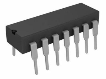
Packaging information: DIP14/SOP14/TSSOP14
Address:Building B4,NO.777,Jianzhu Road,Binhu Distrct,Wuxi City,Jiangsu Province
http://www.i-core. cn
P.C.:214072
2/ 19
VER:2019-05-A1
�Wuxi I-CORE Electronics Co., Ltd.
Tab: 835-12
rev:B3
Number:AiP74HC/HCT164-AX-LJ-A015EN
Ordering Information:
Tube packing specifications:
Type number
Packaging
form
Marking
code
Tube
quantity
Boxed
tube
quantity
Boxed
quantity
Packing
box
number
Packing
quantity
DIP14
74HC164
25
PCS/tube
40
tube/box
1000
PCS/box
10
box/pack
10000
PCS/pack
AiP74HCT164DA.TB
DIP14
74HCT164
25
PCS/tube
40
tube/box
1000
PCS/box
10
box/pack
10000
PCS/pack
AiP74HC164SA.TB
SOP14
74HC164
200
tube/box
10000
PCS/box
5
box/pack
50000
PCS/pack
or
50
PCS/tube
SOP14
74HCT164
50
PCS/tube
200
tube/box
10000
PCS/box
5
box/pack
50000
PCS/pack
AiP74HC164TA.TB
TSSOP14
74HC164
94
PCS/tube
200
tube/box
18800
PCS/box
10
box/pack
188000
PCS/pack
94
PCS/tube
200
tube/box
18800
PCS/box
10
box/pack
188000
PCS/pack
i-c
AiP74HCT164SA.TB
AiP74HCT164TA.TB
TSSOP14
Dimensions of
plastic enclosure:
19.0mm×6.4mm
Pin spacing:
2.54mm
Dimensions of
plastic enclosure:
19.0mm×6.4mm
Pin spacing:
2.54mm
Dimensions of
plastic enclosure:
8.7mm×3.9mm
Pin spacing:
1.27mm
Dimensions of
plastic enclosure:
8.7mm×3.9mm
Pin spacing:
1.27mm
Dimensions of
plastic enclosure:
5.0mm×4.4mm
Pin spacing:
0.65mm
Dimensions of
plastic enclosure:
5.0mm×4.4mm
Pin spacing:
0.65mm
e
AiP74HC164DA.TB
Notes
74HCT164
Address:Building B4,NO.777,Jianzhu Road,Binhu Distrct,Wuxi City,Jiangsu Province
http://www.i-core. cn
P.C.:214072
3/ 19
VER:2019-05-A1
�Wuxi I-CORE Electronics Co., Ltd.
Tab: 835-12
rev:B3
Reel packing specifications:
Packaging
Type number
Marking code
form
Number:AiP74HC/HCT164-AX-LJ-A015EN
Reel
quantity
Boxed reel
quantity
Packing
quantity
SOP14
74HC164
2500
PCS/reel
5000
PCS/box
40000
PCS/pack
AiP74HCT164SA.TR
SOP14
74HCT164
2500
PCS/reel
5000
PCS/box
40000
PCS/pack
AiP74HC164TA.TR
TSSOP14
74HC164
4000
PCS/reel
8000
PCS/box
64000
PCS/pack
AiP74HCT164TA.TR
TSSOP14
74HCT164
4000
PCS/reel
8000
PCS/box
64000
PCS/pack
Dimensions of
plastic enclosure:
8.7mm×3.9mm
Pin spacing:
1.27mm
Dimensions of
plastic enclosure:
8.7mm×3.9mm
Pin spacing:
1.27mm
Dimensions of
plastic enclosure:
5.0mm×4.4mm
Pin spacing:
0.65mm
Dimensions of
plastic enclosure:
5.0mm×4.4mm
Pin spacing:
0.65mm
or
e
AiP74HC164SA.TR
Notes
i-c
Note: If the physical information is inconsistent with the ordering information, please refer to the actual
product.
Address:Building B4,NO.777,Jianzhu Road,Binhu Distrct,Wuxi City,Jiangsu Province
http://www.i-core. cn
P.C.:214072
4/ 19
VER:2019-05-A1
�Wuxi I-CORE Electronics Co., Ltd.
Tab: 835-12
rev:B3
Number:AiP74HC/HCT164-AX-LJ-A015EN
2、Block Diagram And Pin Description
e
2.1、Block Diagram
i-c
or
Figure 1. Logic symbol
Figure 2. IEC logic symbol
Address:Building B4,NO.777,Jianzhu Road,Binhu Distrct,Wuxi City,Jiangsu Province
http://www.i-core. cn
P.C.:214072
5/ 19
VER:2019-05-A1
�Wuxi I-CORE Electronics Co., Ltd.
Tab: 835-12
rev:B3
Number:AiP74HC/HCT164-AX-LJ-A015EN
or
e
Figure 3. Logic diagram
Figure 4. Functional diagram
i-c
2.2、Pin Configurations
2.3、Pin Description
Pin No.
1
2
3
4
5
6
7
Pin Name
DSA
DSB
Q0
Q1
Q2
Q3
GND
Description
data input
data input
output
output
output
output
ground (0V)
Address:Building B4,NO.777,Jianzhu Road,Binhu Distrct,Wuxi City,Jiangsu Province
http://www.i-core. cn
P.C.:214072
6/ 19
VER:2019-05-A1
�Wuxi I-CORE Electronics Co., Ltd.
Tab: 835-12
rev:B3
Number:AiP74HC/HCT164-AX-LJ-A015EN
8
CP
clock input (LOW-to-HIGH, edge-triggered)
9
—
MR
master reset input (active LOW)
10
11
12
13
14
Q4
Q5
Q6
Q7
VCC
output
output
output
output
supply voltage
2.4、Function Table
Operating
modes
Input
—
MR
DSA
DSB
Q0
Q1 to Q7
L to L
q0 to q6
q0 to q6
q0 to q6
q0 to q6
e
L
X
X
X
L
H
↑
l
l
L
H
↑
l
h
L
Shift
H
↑
h
l
L
H
↑
h
h
H
Note: H=HIGH voltage level; L=LOW voltage level; ↑=LOW-to-HIGH clock transition;
h=HIGH voltage level one set-up time prior to the LOW-to-HIGH clock transition;
l=LOW voltage level one set-up time prior to the LOW-to-HIGH clock transition;
q=lower case letters indicate the state of the referenced input one set-up time prior to the
LOW-to-HIGH clock transition.
or
Reset (clear)
CP
Output
3、Electrical Parameter
3.1、Absolute Maximum Ratings
(Voltages are referenced to GND(ground=0V), unless otherwise specified.)
i-c
Parameter
Symbol
Conditions
Min.
supply voltage
VCC
-0.5
input clamping
IIK
VI < -0.5V or VI > VCC+0.5V
current
output clamping
IOK
VO < -0.5V or VO > VCC+0.5V
current
output current
IO
-0.5V < VO < VCC+0.5V
supply current
ICC
ground current
IGND
-50
total power
Ptot
dissipation
storage
Tstg
-65
temperature
DIP
245
Soldering
TL
10s
temperature
SOP
250
Note:
[1] For DIP14 packages: above 70℃ the value of Ptot derates linearly with 12mW/K.
[2] For SOP14 packages: above 70℃ the value of Ptot derates linearly with 8mW/K.
[3] For (T)SSOP14 packages: above 60℃ the value of Ptot derates linearly with 5.5mW/K.
Address:Building B4,NO.777,Jianzhu Road,Binhu Distrct,Wuxi City,Jiangsu Province
http://www.i-core. cn
P.C.:214072
Max.
+7
Unit
V
±20
mA
±20
mA
±25
50
-
mA
mA
mA
500
mW
+150
℃
7/ 19
VER:2019-05-A1
℃
�Wuxi I-CORE Electronics Co., Ltd.
Tab: 835-12
rev:B3
Number:AiP74HC/HCT164-AX-LJ-A015EN
3.2、Recommended Operating Conditions
supply voltage
input voltage
output voltage
VCC
VI
VO
input transition
rise and fall rate
Δt/ΔV
ambient
temperature
Tamb
supply voltage
input voltage
output voltage
VCC
VI
VO
input transition
rise and fall rate
Δt/ΔV
ambient
temperature
Tamb
Conditions
AiP74HC164
VCC=2.0V
VCC=4.5V
VCC=6.0V
AiP74HCT164
VCC=2.0V
VCC=4.5V
VCC=6.0V
Min.
Typ.
Max.
Unit
2.0
0
0
-
5.0
1.67
-
6.0
VCC
VCC
625
139
83
V
V
V
ns/V
ns/V
ns/V
-40
-
+85
℃
4.5
0
0
-
5.0
1.67
-
5.5
VCC
VCC
139
-
V
V
V
ns/V
ns/V
ns/V
+85
℃
Max.
Unit
0.5
1.35
1.8
0.1
0.1
0.1
0.26
0.26
V
V
V
V
V
V
V
V
V
V
V
V
V
V
V
V
±0.1
uA
8
uA
e
Symbol
or
Parameter
-
-40
-
i-c
3.3、Electrical Characteristics
3.3.1、DC Characteristics 1
(Tamb=25℃, voltages are referenced to GND (ground=0V), unless otherwise specified.)
Parameter
Symbol
Conditions
Min. Typ.
AiP74HC164
VCC=2.0V
1.5
1.2
HIGH-level
VCC=4.5V
3.15
2.4
VIH
input voltage
VCC=6.0V
4.2
3.2
0.8
VCC=2.0V
LOW-level
VCC=4.5V
2.1
VIL
input voltage
VCC=6.0V
2.8
IO=-20uA; VCC=2.0V
1.9
2.0
IO=-20uA; VCC=4.5V
4.4
4.5
HIGH-level
VOH
VI = VIH or VIL
IO=-20uA; VCC=6.0V
5.9
6.0
output voltage
IO=-4.0mA; VCC=4.5V
3.98
4.32
IO=-5.2mA; VCC=6.0V
5.48
5.81
0
IO=20uA; VCC=2.0V
IO=20uA; VCC=4.5V
0
LOW-level
VI = VIH or VIL
IO=20uA; VCC=6.0V
0
VOL
output voltage
IO=4.0mA; VCC=4.5V
0.15
IO=5.2mA; VCC=6.0V
0.16
input leakage
VI= VCC or GND;
II
current
VCC=6.0V
VI= VCC or GND; IO=0A;
supply current
ICC
VCC=6.0V
Address:Building B4,NO.777,Jianzhu Road,Binhu Distrct,Wuxi City,Jiangsu Province
http://www.i-core. cn
P.C.:214072
8/ 19
VER:2019-05-A1
�Wuxi I-CORE Electronics Co., Ltd.
Tab: 835-12
HIGH-level
input voltage
LOW-level
input voltage
HIGH-level
output voltage
LOW-level
output voltage
input leakage
current
CI
Number:AiP74HC/HCT164-AX-LJ-A015EN
-
-
3.5
-
pF
AiP74HCT164
VIH
VCC=4.5V to 5.5V
2.0
1.6
-
V
VIL
VCC=4.5V to 5.5V
-
1.2
0.8
V
IO=-20uA; VCC=4.5V
IO=-4.0mA; VCC=4.5V
IO=20uA; VCC=4.5V
VI = VIH or VIL
IO=5.2mA; VCC=6.0V
VI=VCC or GND;
VCC=5.5V
VI=VCC or GND; IO=0A;
VCC=5.5V
per input pin; VI=VCC-2.1V;
IO=0A; other inputs at VCC or GND;
VCC=4.5V to 5.5V
4.4
3.98
-
4.5
4.32
0
0.15
0.1
0.26
V
V
V
V
-
-
±0.1
uA
-
-
8
uA
-
100
360
uA
-
-
3.5
-
pF
VOH
VOL
II
ICC
additional
supply current
ΔICC
input
capacitance
CI
or
supply current
VI = VIH or VIL
e
input
capacitance
rev:B3
3.3.2、DC Characteristics 2
Unit
V
V
V
V
V
V
V
V
V
V
V
V
V
V
V
V
i-c
(Tamb=-40℃ to +85℃, voltages are referenced to GND (ground=0V), unless otherwise specified.)
Parameter
Symbol
Conditions
Min. Typ. Max.
AiP74HC164
1.5
VCC=2.0V
HIGH-level
VIH
VCC=4.5V
3.15
input voltage
VCC=6.0V
4.2
VCC=2.0V
0.5
LOW-level
VIL
VCC=4.5V
1.35
input voltage
VCC=6.0V
1.8
IO=-20uA; VCC=2.0V
1.9
IO=-20uA; VCC=4.5V
4.4
HIGH-level
VI = VIH or VIL
IO=-20uA; VCC=6.0V
5.9
VOH
output voltage
IO=-4.0mA; VCC=4.5V
3.84
IO=-5.2mA; VCC=6.0V
5.34
IO=20uA; VCC=2.0V
0.1
IO=20uA; VCC=4.5V
0.1
LOW-level
VOL
VI = VIH or VIL
IO=20uA; VCC=6.0V
0.1
output voltage
IO=4.0mA; VCC=4.5V
0.33
IO=5.2mA; VCC=6.0V
0.33
input leakage
VI=VCC or GND;
II
±1
current
VCC=6.0V
VI=VCC or GND; IO=0A;
supply current
ICC
80
VCC=6.0V
input
CI
capacitance
Address:Building B4,NO.777,Jianzhu Road,Binhu Distrct,Wuxi City,Jiangsu Province
http://www.i-core. cn
P.C.:214072
uA
uA
pF
9/ 19
VER:2019-05-A1
�Wuxi I-CORE Electronics Co., Ltd.
Tab: 835-12
LOW-level
output voltage
input leakage
current
Number:AiP74HC/HCT164-AX-LJ-A015EN
AiP74HCT164
VIH
VCC=4.5V to 5.5V
2.0
-
-
V
VIL
VCC=4.5V to 5.5V
-
-
0.8
V
IO=-20uA; VCC=4.5V
IO=-4.0mA; VCC=4.5V
IO=20uA; VCC=4.5V
VI = VIH or VIL
IO=5.2mA; VCC=6.0V
VI=VCC or GND;
VCC=5.5V
VI=VCC or GND; IO=0A;
VCC=5.5V
per input pin; VI=VCC-2.1V;
IO=0A; other inputs at VCC or GND;
VCC=4.5V to 5.5V
4.4
3.84
-
-
0.1
0.33
V
V
V
V
-
-
±1
uA
-
-
80
uA
-
-
450
uA
-
-
-
-
pF
VOH
VOL
II
ICC
additional
supply current
ΔICC
input
capacitance
CI
or
supply current
VI = VIH or VIL
e
HIGH-level
input voltage
LOW-level
input voltage
HIGH-level
output voltage
rev:B3
3.3.3、AC Characteristics 1
(Tamb=25℃, voltages are referenced to GND (ground=0V), unless otherwise specified.)
Parameter
CP to Qn
propagation
delay
—
Symbol
tpd
see Figure 6
tPHL
see Figure 7
transition time
tt
see Figure 6
CP
pulse width
tW
see Figure 6
tW
see Figure 7
MR to CP
recovery time
trec
see Figure 7
DSA and DSB
to CP
set-up time
tsu
see Figure 8
i-c
MR to Qn
propagation
delay
Conditions
AiP74HC164
VCC=2.0V
VCC=4.5V
VCC=5.0V;CL=15pF
VCC=6.0V
VCC=2.0V
VCC=4.5V
VCC=5.0V;CL=15pF
VCC=6.0V
VCC=2.0V
VCC=4.5V
VCC=6.0V
VCC=2.0V
VCC=4.5V
VCC=6.0V
VCC=2.0V
VCC=4.5V
VCC=6.0V
VCC=2.0V
VCC=4.5V
VCC=6.0V
VCC=2.0V
VCC=4.5V
VCC=6.0V
—
MR
pulse width
—
Address:Building B4,NO.777,Jianzhu Road,Binhu Distrct,Wuxi City,Jiangsu Province
http://www.i-core. cn
P.C.:214072
Min.
Typ.
Max.
Unit
80
16
14
60
12
10
60
12
10
60
12
10
41
15
12
12
39
14
11
11
19
7
6
14
5
4
17
6
5
17
6
5
8
3
2
170
34
29
140
28
24
75
15
13
-
ns
ns
ns
ns
ns
ns
ns
ns
ns
ns
ns
ns
ns
ns
ns
ns
ns
ns
ns
ns
ns
ns
ns
10/ 19
VER:2019-05-A1
�Wuxi I-CORE Electronics Co., Ltd.
Tab: 835-12
rev:B3
+4
+4
+4
6
30
35
-6
-2
-2
23
71
78
85
-
ns
ns
ns
MHz
MHz
MHz
MHz
-
40
-
pF
VCC=4.5V
-
17
36
ns
VCC=5.0V;CL=15pF
-
14
-
ns
VCC=4.5V
-
19
38
ns
VCC=5.0V;CL=15pF
-
16
-
ns
see Figure 6
VCC=4.5V
-
7
15
ns
tW
see Figure 6
VCC=4.5V
18
7
-
ns
tW
see Figure 7
VCC=4.5V
18
10
-
ns
16
7
-
ns
12
6
-
ns
+4
-2
-
ns
27
55
-
MHz
-
61
-
MHz
-
40
-
pF
DSA and DSB
to CP
hold time
th
see Figure 8
CP
maximum
frequency
fmax
see Figure 6
power
dissipation
capacitance
CPD
CP to Qn
propagation
delay
tpd
see Figure 6
tPHL
see Figure 7
tt
VCC=2.0V
VCC=4.5V
VCC=6.0V
VCC=2.0V
VCC=4.5V
VCC=5.0V;CL=15pF
VCC=6.0V
per package;
VI= GND to VCC
or
e
AiP74HCT164
—
MR to Qn
propagation
delay
transition time
CP
pulse width
Number:AiP74HC/HCT164-AX-LJ-A015EN
—
MR
pulse width
—
i-c
MR to CP
trec
see Figure 7
VCC=4.5V
recovery time
DSA and DSB
tsu
to CP
see Figure 7
VCC=4.5V
set-up time
DSA and DSB
to CP
th
see Figure 8
VCC=4.5V
hold time
CP
VCC=4.5V
maximum
fmax
see Figure 8
VCC=5.0V;CL=15pF
frequency
power
per package;
dissipation
CPD
VI= GND to VCC-1.5V
capacitance
Note:
[1] tpd is the same as tPLH and tPHL.
[2] tt is the same as tTHL and tTLH.
[3] CPD is used to determine the dynamic power dissipation (PD in uW).
PD=(CPD×VCC2×fi×N)+∑(CL×VCC2×fo) where:
fi=input frequency in MHz;
fo=output frequency in MHz;
CL=output load capacitance in pF;
VCC=supply voltage in V;
N=number of inputs switching;
∑(CL×VCC2×fo)=sum of outputs.
Address:Building B4,NO.777,Jianzhu Road,Binhu Distrct,Wuxi City,Jiangsu Province
http://www.i-core. cn
P.C.:214072
11/ 19
VER:2019-05-A1
�Wuxi I-CORE Electronics Co., Ltd.
Tab: 835-12
rev:B3
Number:AiP74HC/HCT164-AX-LJ-A015EN
3.3.4、AC Characteristics 2
(Tamb=-40℃ to +85℃, voltages are referenced to GND (ground=0V), unless otherwise specified.)
Parameter
CP to Qn
propagation
delay
Symbol
tpd
see Figure 6
MR to Qn
propagation
delay
tPHL
see Figure 7
transition time
tt
see Figure 6
CP
pulse width
tW
see Figure 6
Max.
Unit
100
20
17
75
15
13
75
15
13
75
15
13
4
4
4
5
24
28
-
215
43
37
175
35
30
95
19
16
-
ns
ns
ns
ns
ns
ns
ns
ns
ns
ns
ns
ns
ns
ns
ns
ns
ns
ns
ns
ns
ns
ns
ns
ns
ns
ns
MHz
MHz
MHz
MHz
-
-
-
pF
VCC=4.5V
-
-
45
ns
VCC=5.0V;CL=15pF
-
-
-
ns
VCC=4.5V
-
-
48
ns
VCC=5.0V;CL=15pF
-
-
-
ns
or
—
MR
pulse width
tW
see Figure 7
MR to CP
recovery time
trec
see Figure 7
DSA and DSB
to CP
set-up time
tsu
see Figure 8
i-c
—
Typ.
e
—
Min.
Conditions
AiP74HC164
VCC=2.0V
VCC=4.5V
VCC=5.0V;CL=15pF
VCC=6.0V
VCC=2.0V
VCC=4.5V
VCC=5.0V;CL=15pF
VCC=6.0V
VCC=2.0V
VCC=4.5V
VCC=6.0V
VCC=2.0V
VCC=4.5V
VCC=6.0V
VCC=2.0V
VCC=4.5V
VCC=6.0V
VCC=2.0V
VCC=4.5V
VCC=6.0V
VCC=2.0V
VCC=4.5V
VCC=6.0V
VCC=2.0V
VCC=4.5V
VCC=6.0V
VCC=2.0V
VCC=4.5V
VCC=5.0V;CL=15pF
VCC=6.0V
DSA and DSB
to CP
hold time
th
see Figure 8
CP
maximum
frequency
fmax
see Figure 6
power
dissipation
capacitance
CPD
CP to Qn
propagation
delay
tpd
see Figure 6
tPHL
see Figure 7
tt
see Figure 6
VCC=4.5V
-
-
19
ns
tW
see Figure 6
VCC=4.5V
23
-
-
ns
per package;
VI= GND to VCC
AiP74HCT164
—
MR to Qn
propagation
delay
transition time
CP
pulse width
Address:Building B4,NO.777,Jianzhu Road,Binhu Distrct,Wuxi City,Jiangsu Province
http://www.i-core. cn
P.C.:214072
12/ 19
VER:2019-05-A1
�Wuxi I-CORE Electronics Co., Ltd.
Tab: 835-12
rev:B3
Number:AiP74HC/HCT164-AX-LJ-A015EN
—
MR
pulse width
tW
see Figure 7
VCC=4.5V
23
-
-
ns
20
-
-
ns
15
-
-
ns
+4
-
-
ns
22
-
-
MHz
-
-
-
MHz
-
-
-
pF
—
or
e
MR to CP
trec
see Figure 7
VCC=4.5V
recovery time
DSA and DSB
to CP
tsu
see Figure 8
VCC=4.5V
set-up time
DSA and DSB
th
to CP;
see Figure 8
VCC=4.5V
hold time
CP
VCC=4.5V
maximum
fmax
see Figure 6
VCC=5.0V;CL=15pF
frequency
power
per package;
dissipation
CPD
VI= GND to VCC-1.5V
capacitance
Note:
[1] tpd is the same as tPLH and tPHL.
[2] tt is the same as tTHL and tTLH.
[3] CPD is used to determine the dynamic power dissipation (PD in uW).
PD=(CPD×VCC2×fi×N)+∑(CL×VCC2×fo) where:
fi=input frequency in MHz;
fo=output frequency in MHz;
CL=output load capacitance in pF;
VCC=supply voltage in V;
N=number of inputs switching;
∑(CL×VCC2×fo)=sum of outputs.
i-c
4、Testing Circuit
4.1、AC Testing Circuit
Figure 5. Test circuit for measuring switching times
Address:Building B4,NO.777,Jianzhu Road,Binhu Distrct,Wuxi City,Jiangsu Province
http://www.i-core. cn
P.C.:214072
13/ 19
VER:2019-05-A1
�Wuxi I-CORE Electronics Co., Ltd.
Tab: 835-12
rev:B3
Number:AiP74HC/HCT164-AX-LJ-A015EN
Definitions for test circuit:
CL=load capacitance including jig and probe capacitance.
RT=termination resistance should be equal to the output impedance Zo of the pulse generator.
e
4.2、AC Testing Waveforms
i-c
or
Figure 6. Waveforms showing the clock (CP) to output (Qn) propagation delays, the clock pulse width, the
output transition times and the maximum clock frequency
Figure 7. Waveforms showing the master reset (MR) pulse width, the master reset to output (Qn)
propagation delays and the master reset to clock (CP) removal time
Address:Building B4,NO.777,Jianzhu Road,Binhu Distrct,Wuxi City,Jiangsu Province
http://www.i-core. cn
P.C.:214072
14/ 19
VER:2019-05-A1
�Wuxi I-CORE Electronics Co., Ltd.
rev:B3
Number:AiP74HC/HCT164-AX-LJ-A015EN
e
Tab: 835-12
Figure 8. Waveforms showing the data set-up and hold times for Dn inputs
4.3、Measurement Points
Input
VM
0.5×VCC
1.3V
VM
0.5×VCC
1.3V
Output
VX
0.1×VCC
0.1×VCC
VY
0.9×VCC
0.9×VCC
or
Type
AiP74HC164
AiP74HCT164
4.4、Test Data
Type
VI
VCC
3.0V
Load
tr , tf
6.0ns
6.0ns
i-c
AiP74HC164
AiP74HCT164
Input
CL
15pF, 50pF
15pF, 50pF
Address:Building B4,NO.777,Jianzhu Road,Binhu Distrct,Wuxi City,Jiangsu Province
http://www.i-core. cn
P.C.:214072
Test
tPLH, tPHL
tPLH, tPHL
15/ 19
VER:2019-05-A1
�Wuxi I-CORE Electronics Co., Ltd.
Tab: 835-12
rev:B3
Number:AiP74HC/HCT164-AX-LJ-A015EN
5、Package Information
i-c
or
e
5.1、DIP14
Address:Building B4,NO.777,Jianzhu Road,Binhu Distrct,Wuxi City,Jiangsu Province
http://www.i-core. cn
P.C.:214072
16/ 19
VER:2019-05-A1
�Wuxi I-CORE Electronics Co., Ltd.
Tab: 835-12
rev:B3
Number:AiP74HC/HCT164-AX-LJ-A015EN
i-c
or
e
5.2、SOP14
Address:Building B4,NO.777,Jianzhu Road,Binhu Distrct,Wuxi City,Jiangsu Province
http://www.i-core. cn
P.C.:214072
17/ 19
VER:2019-05-A1
�Wuxi I-CORE Electronics Co., Ltd.
Tab: 835-12
rev:B3
Number:AiP74HC/HCT164-AX-LJ-A015EN
i-c
or
e
5.3、TSSOP14
Address:Building B4,NO.777,Jianzhu Road,Binhu Distrct,Wuxi City,Jiangsu Province
http://www.i-core. cn
P.C.:214072
18/ 19
VER:2019-05-A1
�Wuxi I-CORE Electronics Co., Ltd.
Tab: 835-12
rev:B3
Number:AiP74HC/HCT164-AX-LJ-A015EN
6、Statements And Notes
6.1、The name and content of Hazardous substances or Elements in the product
Hazardous substances or Elements
Lead
and
lead
compou
nds
Mercur
y and
mercur
y
compo
unds
Cadm
ium
and
cadmi
um
comp
ounds
Lead frame
○
○
○
○
○
Plastic resin
○
○
○
○
Chip
○
○
○
The lead
○
○
○
Plastic sheet
installed
○
○
○
Polybro
minate
d
biphen
yl
ethers
Dibutyl
phthala
te
Butylbe
nzyl
phthala
te
Di-2-et
hylhex
yl
phthala
te
Diisobu
tyl
phthala
te
○
○
○
○
○
○
○
○
○
○
○
○
○
○
○
○
○
○
○
○
○
○
○
○
○
Polybro
minated
biphenyl
s
e
Part name
Hexaval
ent
chromiu
m
compoun
ds
○
○
○
○
○
○
○
○:Indicates that the content of hazardous substances or elements in the detection limit
of the following the SJ/T11363-2006 standard。
×:Indicates that the content of hazardous substances or elements exceeding the SJ/T11363-2006
Standard limit requirements。
or
explanation
6.2、Notion
Recommended carefully reading this information before the use of this product;
The information in this document are subject to change without notice;
i-c
This information is using to the reference only, the company is not responsible for any loss;
The company is not responsible for the any infringement of the third party patents or other rights of
the responsibility.
Address:Building B4,NO.777,Jianzhu Road,Binhu Distrct,Wuxi City,Jiangsu Province
http://www.i-core. cn
P.C.:214072
19/ 19
VER:2019-05-A1
�