WPM2087
WPM2087
Single P-Channel, -20V, -4.3A, Power MOSFET
VDS (V)
Http://www.sh-willsemi.com
Typical RDS(on) (mΩ)
34@ VGS=-4.5V
-20
39 @ VGS=-3.1V
45 @ VGS=-2.5V
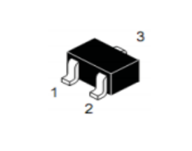
SOT-23
Descriptions
D
The WPM2087 is P-Channel
3
enhancement MOS
Field Effect Transistor. Uses advanced trench
technology and design to provide excellent RDS(ON)
with low gate charge. This device is suitable for use
in DC-DC conversion, power switch and charging
circuit. Standard Product WPM2087 is Pb-free.
1
2
G
S
Pin configuration (Top view)
Features
Trench Technology
Supper high density cell design
Excellent ON resistance
Extremely Low Threshold Voltage
Small package SOT-23
Applications
PE
= Device Code
Y
= Year
W
= Week(A~z)
Marking
DC/DC converters
Power supply converters circuit
Load/Power Switching for portable device
Will Semiconductor Ltd.
Order information
1
Device
Package
Shipping
WPM2087-3/TR
SOT-23
3000/Tape&Reel
July.2016- Rev.1.0
�WPM2087
Absolute Maximum ratings
Parameter
Symbol
10 s
Steady State
Drain-Source Voltage
VDS
-20
Gate-Source Voltage
VGS
±12
Continuous Drain Current
ad
Maximum Power Dissipation a d
Continuous Drain Current b d
Maximum Power Dissipation b d
T A=25°C
ID
T A=70°C
T A=25°C
PD
T A=70°C
T A=25°C
ID
T A=70°C
T A=25°C
PD
T A=70°C
Unit
V
-4.3
-3.6
-3.4
-2.9
1.2
0.9
0.8
0.6
-3.4
-3.1
-2.7
-2.5
0.8
0.7
0.5
0.4
A
W
A
W
Pulsed Drain Current c
IDM
-18
A
Operating Junction Temperature
TJ
-55 to 150
°C
Lead Temperature
TL
260
°C
Storage Temperature Range
T stg
-55 to 150
°C
Thermal resistance ratings
Parameter
Junction-to-Ambient Thermal Resistance a
Junction-to-Ambient Thermal Resistance b
Junction-to-Case Thermal Resistance
Symbol
t ≤ 10 s
Steady State
t ≤ 10 s
Steady State
Steady State
RθJA
RθJA
RθJC
Typical
Maximum
84
102
120
145
130
160
145
190
60
75
a.
Surface mounted on FR4 Board using 1 in sq pad size, 1oz Cu.
b.
Surface mounted on FR4 board using the minimum recommended pad size, 1oz Cu.
c.
Repetitive rating, pulse width limited by junction temperature, tp=10µs, Duty Cycle=1%.
d.
Repetitive rating, pulse width limited by junction temperature TJ(MAX)=150°C.
Will Semiconductor Ltd.
2
Unit
°C/W
July.2016- Rev.1.0
�WPM2087
Electronics Characteristics (Ta=25oC, unless otherwise noted)
Parameter
Symbol
Test Conditions
Min
Typ
Max
Unit
OFF CHARACTERISTICS
Drain-to-Source Breakdown Voltage
BVDSS
VGS = 0 V, ID = -250uA
Zero Gate Voltage Drain Current
IDSS
VDS =-16V, VGS = 0V
Gate-to-source Leakage Current
IGSS
VDS = 0 V, VGS = ±12V
VGS(TH)
VGS = VDS, ID = -250uA
-20
V
-1
uA
±100
nA
-0.75
-1.0
V
VGS = -4.5V, ID = -5A
34
45
VGS =-3.1V, ID = -2.5A
39
55
VGS =-2.5V, ID = -2.0A
45
59
VDS = -5 V, ID = -3.0A
4
9
ON CHARACTERISTICS
Gate Threshold Voltage
Drain-to-source On-resistance
Forward Transconductance
RDS(on)
gFS
-0.4
mΩ
S
CHARGES, CAPACITANCES AND GATE RESISTANCE
Input Capacitance
CISS
1182
Output Capacitance
COSS
Reverse Transfer Capacitance
CRSS
Total Gate Charge
QG(TOT)
Threshold Gate Charge
QG(TH)
VGS = -4.5 V, VDS = -10 V,
0.85
Gate-to-Source Charge
QGS
ID =-5.0 A
2.5
Gate-to-Drain Charge
QGD
2.8
Turn-On Delay Time
td(ON)
7.8
Rise Time
tr
VGS = -10 V, VDS =-15 V,
6.4
Turn-Off Delay Time
td(OFF)
ID=-5A, RG=6Ω
80
Fall Time
tf
VGS = 0 V, f = 1.0MHz, VDS =
126
-10 V
pF
108
12
nC
SWITCHING CHARACTERISTICS
ns
18
BODY DIODE CHARACTERISTICS
Forward Voltage
Will Semiconductor Ltd.
VSD
VGS = 0 V, IS = -1A
3
-0.6
-0.75
-1.2
V
July.2016- Rev.1.0
�WPM2087
20
Typical Characteristics (Ta=25oC, unless otherwise noted)
20
20
VGS=-6V
VGS=-4.5V
16
VGS=-3.5V
12
VGS=-2.5V
8
4
0
0
1
2
12
o
10
150 C
8
6
o
25 C
4
o
-50 C
2
1.0
1.5
2.0
-VDS-Drain to Source Voltage(V)
-VGS-Gate to Source Voltage(V)
Output characteristics
Transfer characteristics
2.5
0.20
VGS=-2.5V
0.05
VGS=-3.5V
VGS=-4.5V
0.04
0.03
VGS=-6V
4
8
12
16
ID=-5A
0.16
0.12
0.08
0.04
0.00
20
2
3
4
5
6
-IDS-Drain to Source Current(A)
-VGS-Gate to Source Voltage (V)
On-Resistance vs. Drain current
On-Resistance vs. Gate-to-source voltage
VGS=-4.5V
ID=-5A
1.2
0.9
0.6
-50
14
0
0.5
0.06
1.5
16
3
0.07
0.02
VDS=-5V
18
-IDS-Drain Source Current(A)
15
RDS(ON)-On-Resistance()
VGS=5.5V
10
Gate Threshold Voltage Normalized
VGS=6V
5
VDS-Drain-to-Source Voltage(V)
-IDS-Drain to Source Current(A)
=8V
GS
0
RDS(ON)-On Resistance()
VGS=10VV
0
RDS(ON)-On-Resistance Normalized
IDS-Drain-to-Source Current (A)
6
4
2
0
50
100
150
ID=-250uA
1.2
1.0
0.8
0.6
0.4
-50
0
50
100
150
o
Temperature ( C)
o
Temperature ( C)
Threshold voltage vs. Temperature
On-Resistance vs. Junction temperature
Will Semiconductor Ltd.
1.4
4
July.2016- Rev.1.0
�WPM2087
2000
10
-ISD-Source to Drain Current (A)
Capacitance (pF)
F = 1MHZ
Ciss
1500
1000
Coss
500
Crss
0
0
3
6
9
12
8
6
2
0.0
15
o
T=25 C
o
T=150 C
4
0.2
0.4
0.6
0.8
1.0
1.2
-VSD-Source to Drain Voltage (V)
-VDS-Drain to Source Voltage (V)
Body diode forward voltage
Capacitance
100
o
100
TJ(MAX)=150 C
o
-ID-Drain Current (A)
TA=25 C
Power (W)
80
60
40
Limit by Rdson
10
100us
1
1ms
10s
10ms
0.1
20
100ms
1s
DC
o
TA=25 C
Single Pulse
0
1E-4
1E-3
0.01
0.1
1
10
0.01
0.1
100
1
10
100
-VDS-Drain to Source Voltage(V)
Pulse width (S)
*VGS>minimum VGS at which RDS(ON) is specified
Safe operating power
Single pulse power
-VGS-Gate to Source Voltage (V)
4.5
VDS=-10V
ID=-5A
3.0
1.5
0.0
0
3
9
6
12
15
Qg(nC)
Gate Charge Characteristics
Will Semiconductor Ltd.
5
July.2016- Rev.1.0
�WPM2087
2
1
Normalized Effective Transient
Thermal Impedance
Duty Cycle = 0.5
0.1
0.2
Notes:
0.1
PDM
0.05
t1
t2
1. Duty Cycle, D =
0.02
t1
t2
2. Per Unit Base = RthJA = 145_C/W
3. TJM - TA = PDMZthJA(t)
4. Surface Mounted
Single Pulse
0.01
10 -4
10 -3
10 -2
10 -1
1
10
100
600
Square Wave Pulse Duration (sec)
Transient thermal response (Junction-to-Ambient)
Will Semiconductor Ltd.
6
July.2016- Rev.1.0
�WPM2087
Package outline dimensions
SOT-23
Symbol
Dimensions In Millimeters
Min.
Max.
A
0.900
1.150
A1
0.000
0.100
A2
0.900
1.050
b
0.300
0.500
c
0.080
0.150
D
2.800
3.000
E
1.200
1.400
E1
2.250
2.550
e
e1
0.950 (Typ.)
1.800
2.000
L
L1
ș
Will Semiconductor Ltd.
0.550 (Typ.)
0.300
0
0.500
o
8o
7
July.2016- Rev.1.0
�
很抱歉,暂时无法提供与“WPM2087-3/TR”相匹配的价格&库存,您可以联系我们找货
免费人工找货- 国内价格
- 1+0.57530
- 200+0.37070
- 1500+0.32230
- 3000+0.28600
- 国内价格
- 5+0.46749
- 20+0.42625
- 100+0.38500
- 500+0.34375
- 1000+0.32450
- 2000+0.31075