WL2863E
WL2863E
Ultra-Low Noise, High PSRR LDO, 250mA Linear
http://www.omnivision-group.com
Regulator for RF and Analog Circuits
Descriptions
The WL2863E is a linear regulator capable of
supplying 250-mA output current. Designed to meet
the requirements of RF and analog circuits, the
WL2863E device provides low noise, high PSRR, low
quiescent current and very good load /line transients.
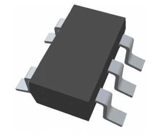
SOT-23-5L
The device is designed to work with a 1μF input and
1μF output ceramic capacitor (no separate noise
Operation bypass capacitor is required).
The WL2863E regulators are available in standard
SOT-23-5L Package. Standard products are Pb-free
and Halogen-free.
Features
Input Voltage Range
:2.2V~5.5V
Output Voltage Range
:1.2V~4.3V
Output current
:250mA
PSRR
:Typ.100dB at 10mA,f =1KHz
Pin Configuration (Top View)
:Typ. 45dB at 10mA , f =1MHz
Low Dropout
:Typ. 115mV at 250mA
Quiescent current
:Typ. 21μA
Low Output Voltage Noise:Typ. 7μVRMS
Output Voltage Tolerance :±2%
Shutdown Current
:Typ. 0.01μA
UVLO Threshold(V)
:Typ. 1.90V
Recommend capacitor
:1uF
Stable with 1μF Ceramic Input and Output capacitor
No Noise Bypass Capacitor Required
Thermal-Overload Protection
Marking
2863 : Device Code
E : Special Code
*
Applications
Cell phones , radiophone, digital cameras
Bluetooth, wireless handsets
HiFi products
Others portable electronics device
Will Semiconductor Ltd.
Y
: Voltage Code
: Year Code
W : Week Code
Order Information
For detail order information, please see page 11
1
Dec, 2021
– Rev 1.1
�WL2863E
Typical Application
VIN
VIN
VOUT
VOUT
1uF
1uF
WL2863
ON
OFF
EN
GND
Note : The input and output capacitor must be located a distance of not more than 1 cm
PIN Functions
PIN
Symbol
1
VIN
2
GND
3
EN
4
NC
5
VOUT
Description
Input voltage supply pin , 1μF capacitor should be
connected at this input
Common ground connection
Chip enable: Applying VEN < 0.4 V disables the regulator,
Pulling VEN > 1.2 V enables the LDO.
No internal electrical connection
Regulated output voltage. 1μF capacitor should be
connected at this input
Block Diagram
Will Semiconductor Ltd.
2
Dec, 2021
– Rev 1.1
�WL2863E
Absolute Maximum Ratings
Parameter
Value
Power Dissipation, PD@TA=25℃
Internally Limited
VIN Range
-0.3~6.0
V
VEN Range
−0.3 to VIN + 0.3
V
VOUT Range
−0.3 to VIN + 0.3
V
IOUT
250
Lead Temperature Range
260
Moisture Sensitivity Level
Level-3
Storage Temperature Range
-55 ~ 150
o
Operating Junction Temperature Range
150
o
ESD Ratings
Unit
mW
mA
C
o
C
C
HBM
2000
V
MM
200
V
Recommend Operating Ratings
Parameter
Operating Input Voltage Range
Value
Unit
2.2~5.5
(1)
Operating Output Voltage Range
1.2~4.3
Operating Temperature Range
-40~85
Thermal Resistance, RθJA
250
V
V
C
o
C/W
o
(1) In order to achieve high performance of PSRR, it is recommended that the VIN needs to be no smaller
than (VOUT+0.5V).
Will Semiconductor Ltd.
3
Dec, 2021
– Rev 1.1
�WL2863E
Electronics Characteristics (VIN=VOUT(NOM)+1V, CIN=COUT=1uF, VEN = 1.2 V. Typical values are at Ta =
+25°C ,unless otherwise noted)
Parameter
Symbol
Operating Input Voltage
VIN
Output Voltage Accuracy
VOUT
Output Current Limit
ILIM
Dropout Voltage
Condition
VIN = VOUT(NOM) + 1 V
IOUT=1mA
VOUT = 90% VOUT(NOM)
Min.
Typ.
Max.
Unit
2.2
5.5
V
-2
+2
%
250
mA
VOUT=2.8V(NOM), IOUT=250mA
115
170
VOUT=3.0V(NOM), IOUT=250mA
108
162
VOUT=3.3V(NOM), IOUT=250mA
102
150
mV
Line Regulation
△VLINE
VIN=2.2V~5V ,IOUT=1mA
0.1
mV
Load Regulation
△VLoad
IOUT=1~200mA
15
mV
Quiescent Current
IQ
IOUT=0mA
21
Short Current
ISHORT
VOUT=0V
390
Shut-down Current
ISHDN
VEN
0.01
Power Supply Rejection
Rate
PSRR
0.4 V, VIN = 4.8 V
IOUT =10mA
f=100Hz
95
f=1KHz
100
f=100KHz
60
f=1MHz
45
EN logic high voltage
VENH
VIN=5.5V, IOUT=1mA
EN logic low voltage
VENL
VIN=5.5V, VOUT=0V
EN Input Current
IEN
VEN = 0 to 5.5V
μA
mA
1.0
μA
dB
1.2
COUT = 1μF, From assertion of
Turn−On Time
25
V
0.4
V
1
μA
1.5
VEN to VOUT = 95% VOUT (NOM)
IOUT =1mA
7
IOUT =200mA
5
mS
Output Voltage Noise
eNO
10Hz to 100KHz,
Thermal shutdown
TSDH
Temperature rising
150
o
threshold
TSDL
Temperature falling
120
o
Under voltage lock out
threshold
Active Output Discharge
Resistance
VUVLO
RLOW
VEN
很抱歉,暂时无法提供与“WL2863E28-5/TR”相匹配的价格&库存,您可以联系我们找货
免费人工找货- 国内价格
- 5+0.51001
- 20+0.46501
- 100+0.42001
- 500+0.37500
- 1000+0.35400
- 2000+0.33900
- 国内价格
- 5+0.80180
- 50+0.63375
- 150+0.54983
- 500+0.48687
