UMW
R
UMW 20N06
60V N-Channel Enhancement Mode Power MOSFET
General Description
The 20N06 uses advanced trench technology and design to
provide excellent R DS(ON) wi th low gate charge. It can be
used in a wide variety of applications.
Features
VDS = 60V,ID =20A
RDS(ON),23mΩ(Typ) @ VGS =10V
RDS(ON),29mΩ(Typ) @ VGS =4.5V
Advanced Trench Technology
Excellent RDS(ON) and Low Gate Charge
Lead free product is acquired
Application
Load
Switch
PWM Application
Power management
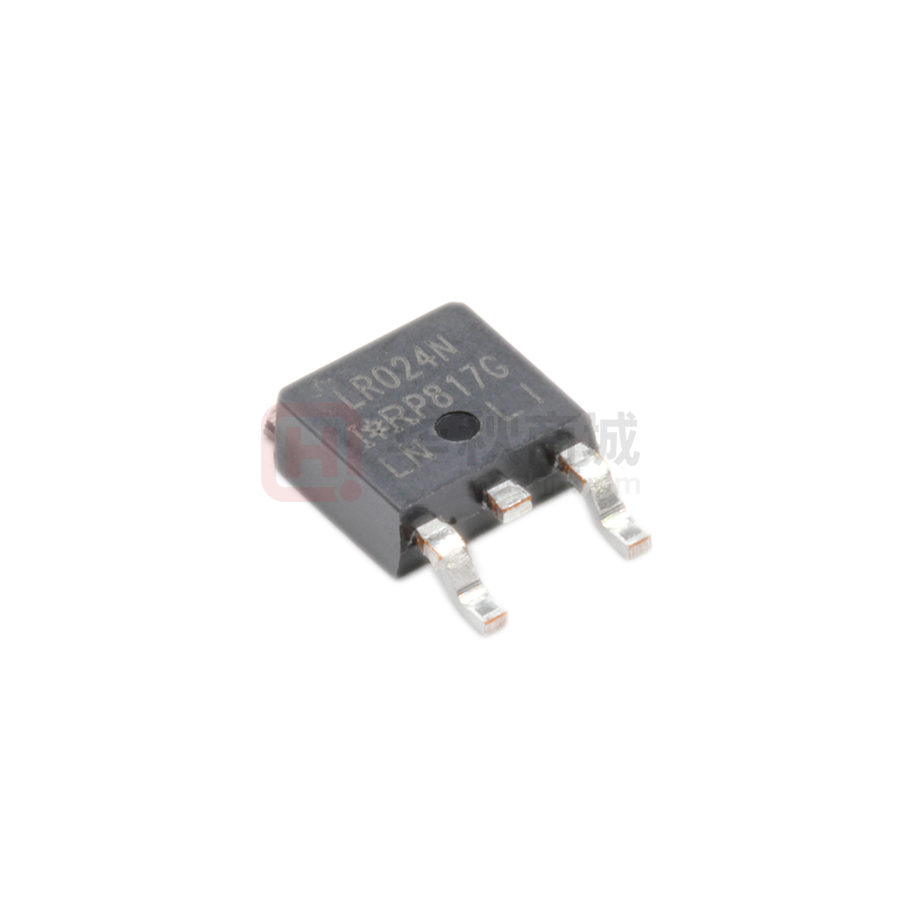
Package Marking and Ordering Information
Device Marking
Device
Device Package
UMW 20N06
UMW 20N06
TO-252
Reel Size
Tape width
330mm
Quantity
12mm
2500
Absolute Maximum Ratings(TA=25℃ unless otherwise noted)
Parameter
Symbol
Value
Unit
Drain-Source Voltage
VDS
60
V
Gate-Source Voltage
VGS
±20
V
20
A
14
A
IDM
120
A
EAS
72
mJ
PD
55
W
TSTG
-55 to +150
℃
TJ
-55 to +150
℃
Drain Current-ContinuousNote3
TC=25℃
TC=100℃
Drain Current-PulsedNote1
Avalanche EnergyNote4
Maximum Power Dissipation
TC=25℃
Storage Temperature Range
Operating Junction Temperature Range
ID
Thermal Resistance
Parameter
Thermal Resistance,Junction-to-Case
www.umw-ic.com
Symbol
Min.
Typ.
Max
Unit
RθJC
-
-
2.7
℃/W
1
友台半导体有限公司
�UMW
R
UMW 20N06
60V N-Channel Enhancement Mode Power MOSFET
Electrical Characteristics(TJ=25℃ unless otherwise noted)
OFF CHARACTERISTICS
Parameter
Symbol
Conditions
Min.
Typ.
Max.
Unit
Drain-Source Breakdown Voltage
BVDSS
VGS=0V,IDS=250uA
60
-
-
V
Zero Gate Voltage Drain Current
IDSS
VDS=60V,VGS=0V
-
-
1
uA
Gate-Body Leakage
IGSS
VGS=±20V,VDS=0V
-
-
±100
nA
Symbol
Conditions
Min.
Typ.
Max.
Unit
Gate Threshold Voltage
VGS(TH)
VDS=VGS,IDS=250uA
1.0
1.6
2.5
V
Drain-Source On-State Resistance
RDS(ON)
VGS=10V,IDS=15A
-
23
29
mΩ
VGS=4.5V,IDS=10A
-
29
40
mΩ
Conditions
Min.
Typ.
Max.
Unit
-
1562
-
-
75.4
-
-
66.8
-
Min.
Typ.
Max.
-
7.5
-
-
21
-
-
16
-
-
23.5
-
-
25
-
-
4.5
-
-
6.5
-
ON CHARACTERISTICS
Parameter
DYNAMIC CHARACTERISTICS
Parameter
Symbol
Input Capacitance
CiSS
Output Capacitance
COSS
Reverse Transfer Capacitance
Crss
VDS =25V, VGS = 0V,
f=1MHz
pF
SWITCHING CHARACTERISTICS
Parameter
Turn-On Delay Time
Rise Time
Symbol
Td(on)
tr
Turn-Off Delay Time
Fall Time
Conditions
VGS=10V,VDs=30V,
RGEN=1.8Ω
Td(off)
ID=15A
tf
Total Gate Charge at 10V
Qg
Gate to Source Gate Charge
Qgs
Gate to Drain“Miller”Charge
Qgd
VDS=30V,IDS=15A,
VGS=10V
Unit
ns
nC
DRAIN-SOURCE DIODE CHARACTERISTICS AND MAXIMUM RATINGS
Parameter
Symbol
Conditions
Min.
Typ.
Max.
Unit
VSD
VGS=0V,IDS=15A
-
-
1.2
V
Reverse Recovery Time
trr
TJ=25℃,IF=15A
-
29
-
nS
Reverse Recovery Charge
Qrr
di/dt=100A/us
-
45
-
nC
Drain-Source Diode Forward Voltage
Notes:
1: Repetitive rating, pulse width limited by maximum junction temperature.
2: Surface mounted on FR4 Board, t≤10sec.
3: Pulse width ≤ 300μs, duty cycle ≤ 2%.
4: EAS condition: L=0.5mH,VDD=30V,VG=10V,VGATE=60V,Start TJ=25℃.
www.umw-ic.com
2
友台半导体有限公司
�UMW
R
www.umw-ic.com
UMW 20N06
60V N-Channel Enhancement Mode Power MOSFET
3
友台半导体有限公司
�UMW
R
www.umw-ic.com
UMW 20N06
60V N-Channel Enhancement Mode Power MOSFET
4
友台半导体有限公司
�UMW
R
www.umw-ic.com
UMW 20N06
60V N-Channel Enhancement Mode Power MOSFET
5
友台半导体有限公司
�UMW
R
www.umw-ic.com
UMW 20N06
60V N-Channel Enhancement Mode Power MOSFET
6
友台半导体有限公司
�
很抱歉,暂时无法提供与“20N06”相匹配的价格&库存,您可以联系我们找货
免费人工找货- 国内价格
- 5+0.70697
- 50+0.55426
- 150+0.47790
- 500+0.42066
- 2500+0.34690
- 5000+0.32400
- 国内价格
- 1+0.60486
- 100+0.40392
- 1250+0.36618
- 2500+0.33660
- 国内价格
- 5+0.67414
- 50+0.53557
- 500+0.41434
- 1000+0.40812
- 2500+0.34741