TSH248
Micropower Omni-Polar Hall Effect Switch
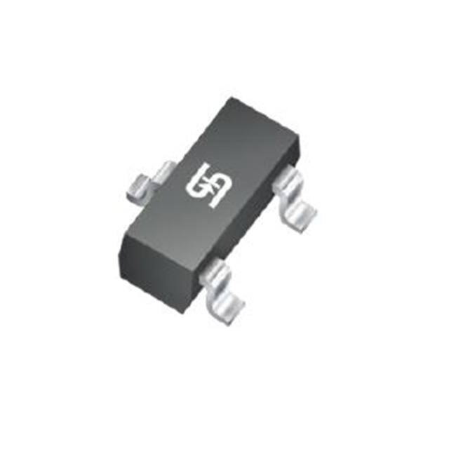
TSOT-23
Pin Definition:
1. VCC
2. Output
3. GND
Description
TSH248 Hall-effect sensor is a temperature stable, stress-resistant, micro-power switch. Superior hightemperature performance is made possible through a dynamic offset cancellation that utilizes chopperstabilization. This method reduces the offset voltage normally caused by device over-molding, temperature
dependencies and thermal stress.
TSH248 includes the following on a single silicon chip: voltage regulator, Hall voltage generator, small-signal
amplifier, chopper stabilization, Schmitt trigger, open-drain output. Advanced CMOS wafer fabrication processing
is used to take advantage of low-voltage requirements, component matching, very low input-offset errors and
small component geometries.
Features
●
CMOS Hall IC Technology
●
Solid-State Reliability
●
Low power consumption for battery applications
●
Operation voltage range from 2.5V~3.5V
Ordering Information
Part No.
TSH248CX RFG
Package
Packing
TSOT-23
3kpcs / 7” Reel
Note: “G” denote for Halogen Free Product
Application
●
Solid state switch
●
Lid close sensor for power supply devices
●
Magnet proximity sensor for reed switch
replacement in high duty cycle applications.
●
Handheld Wireless Handset Awake Switch (Flip
Cell/PHS Phone/Note Book/Flip Video Set)
Absolute Maximum Ratings (TA = 25oC unless otherwise noted)
Characteristics
Limit
Value
Unit
Supply voltage
VCC
5
V
Output Voltage
VOUT
5
V
Reverse voltage
VCC/OUT
-0.3
V
Unlimited
G
mA
Magnetic flux density
Output current
IOUT
2
Operating Temperature Range
TOPR
-40 to +85
Storage temperature range
TSTG
Maximum Junction Temp
Thermal Resistance - Junction to Ambient
Thermal Resistance - Junction to Case
Package Power Dissipation
o
C
o
C
-55 to +150
o
C
TJ
150
RθJA
543
o
RθJC
410
o
PD
230
C/W
C/W
mW
Note: Exceeding the absolute maximum ratings may cause permanent damage. Exposure to absolute maximumrated conditions for extended periods may affect device reliability.
1/8
Version: B14
�TSH248
Micropower Omni-Polar Hall Effect Switch
Block Diagram
Note: Static sensitive device; please observe ESD precautions. Reverse VCC protection is not included. For reverse
voltage protection, a 100Ω resistor in series with VCC is recommended.
Typical Application Circuit
C1:10nF
C2:100pF
R1:100kΩ
2/8
Version: B14
�TSH248
Micropower Omni-Polar Hall Effect Switch
Electrical Specifications (DC Operating Parameters: TA=+25oC, VCC=3V)
Parameters
Test Conditions
Min
Typ
Max
Units
2.5
--
3.5
V
Awake State
--
2.5
4.0
mA
Sleep State
--
8.0
12
µA
Average
--
10
16
µA
Output Low Voltage
IOUT=1mA
--
--
0.3
V
Output Leakage Current
Output off
--
--
1
µA
Awake Mode Time
Operating
--
70
--
µs
Sleep Mode Time
Operating
--
70
--
ms
--
0.1
--
%
Min.
Typ.
Max.
Units
Supply Voltage
Operating
Supply Current
Duty Cycle
Magnetic Specifications
o
DC Operating Parameters TA=25 C, VCC=3.0V
Parameter
Symbol
Test Conditions
Operating
Point
BOPS
N pole to branded side, B > BOP, VOUT On
6
--
60
G
BOPN
S pole to branded side, B > BOP, VOUT On
-60
--
-6
G
Release
Point
BRPS
N pole to branded side, B < BRP, VOUT Off
5
--
-59
G
BRPN
S pole to branded side, B < BRP, VOUT Off
-60
--
-5
G
Hysteresis
BHYS
|BOPx - BRPx|
--
7
--
G
Note: 1G (Gauss) = 0.1mT (millitesla)
3/8
Version: B14
�TSH248
Micropower Omni-Polar Hall Effect Switch
Output Behavior versus Magnetic Pole
o
DC Operating Parameters: TA = -40 to 85 C, VCC = 2.5V ~ 3.5V
Parameter
Test condition
OUT
South pole
B
很抱歉,暂时无法提供与“TSH248CX RFG”相匹配的价格&库存,您可以联系我们找货
免费人工找货