TSH188
Ultra High Sensitivity Hall Effect Latch
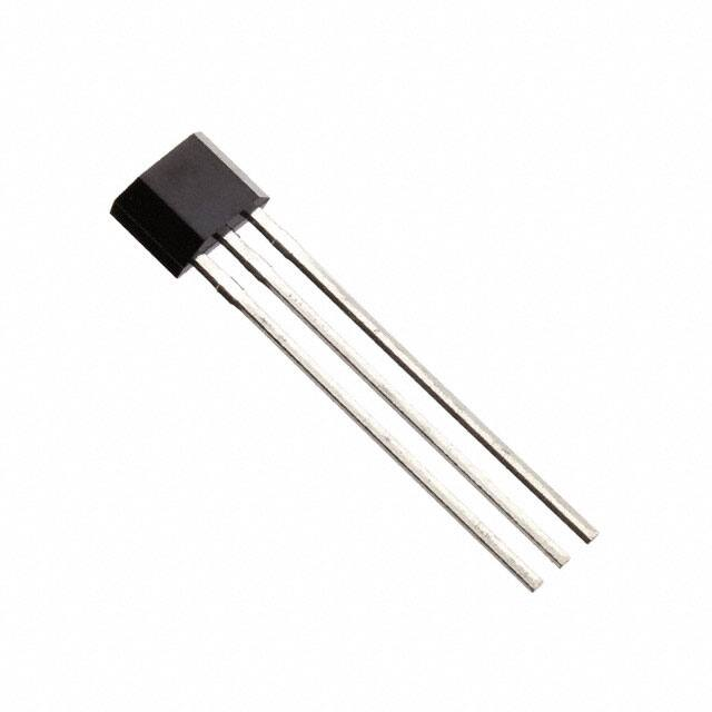
TO-92S
Pin Definition:
1. VCC
2. GND
3. Output
SOT-23
Pin Definition:
1. VCC
2. Output
3. GND
Description
TSH188 Hall-effect sensor is a temperature stable, stress-resistant sensor. Superior high-temperature
performance is made possible through a dynamic offset cancellation that utilizes chopper-stabilization. This
method reduces the offset voltage normally caused by device over molding, temperature dependencies, and
thermal stress. TSH188 includes the following on a single silicon chip: voltage regulator, Hall voltage generator,
small-signal amplifier, chopper stabilization, Schmitt trigger. Advanced DMOS wafer fabrication processing is used
to take advantage of low-voltage requirements, component matching, very low input-offset errors, and small
component geometries. This device requires the presence of both south and north polarity magnetic fields for
operation. In the presence of a south polarity field of sufficient strength, the device output sensor on, and only
switches off when a north polarity field of sufficient strength is present
Features
●
●
●
●
●
Ordering Information
o
100% tested at 125 C
Temperature compensation function
Chopper stabilized amplifier stage.
Optimized for BLDC motor applications.
Reliable and low shifting on high Temp condition.
TSH188CT B0G
TSH188CT A3G
TSH188CX RFG
Package
Packing
TO-92S
TO-92S
SOT-23
1Kpcs / Bulk Bag
2Kpcs / Ammo
3Kpcs / 7” Reel
Note: “G” denote for Halogen Free Product
Application
●
●
●
●
●
●
Part No.
High temperature Fan motor
3 phase BLDC motor application
Speed sensing, Position sensing, Current sensing
Revolution counting
Solid-State Switch
Linear/Angular Position Detection
Absolute Maximum Rating (Ta = 25oC unless otherwise noted)
Characteristics
Supply voltage
Output Voltage
Reverse voltage
Magnetic flux density
Output current
Operating Temperature Range
Storage temperature range
Maximum Junction Temp
Thermal Resistance - Junction to Ambient
Thermal Resistance - Junction to Case
Package Power Dissipation
Note: Do not apply reverse voltage to VCC and VOUT
Limit
Value
Unit
VCC
VOUT
VCC/OUT
28
28
-28
Unlimited
50
V
V
V
Gauss
mA
o
C
IOUT
TOPR
-40 to +125
o
-55 to +150
TSTG
C
o
150
TJ
C
206
TO-92S
o
θJA
C/W
543
SOT-23
148
TO-92S
o
θJC
C/W
410
SOT-23
606
TO-92S
PD
mW
230
SOT-23
Pin, It may be caused for Miss function or damaged device.
1/8
Version: C13
�TSH188
Ultra High Sensitivity Hall Effect Latch
Block Diagram
Typical Application Circuit
C1:10nF
C2:1nF
R1:1KΩ
Electrical Specifications (DC Operating Parameters:TA=+25oC,VCC=12V)
Parameters
Test Conditions
Min
Typ
Max
Units
2.5
--
24
V
Supply Voltage
Operating
Supply Current
BBOP
--
--
400
mV
Output Leakage Current
IOFF BBOP
Open(Hi)
Low
South pole
B
很抱歉,暂时无法提供与“TSH188CT B0G”相匹配的价格&库存,您可以联系我们找货
免费人工找货- 国内价格 香港价格
- 50000+4.8847950000+0.63317