TSH181
General Purpose Hall Effect Latch
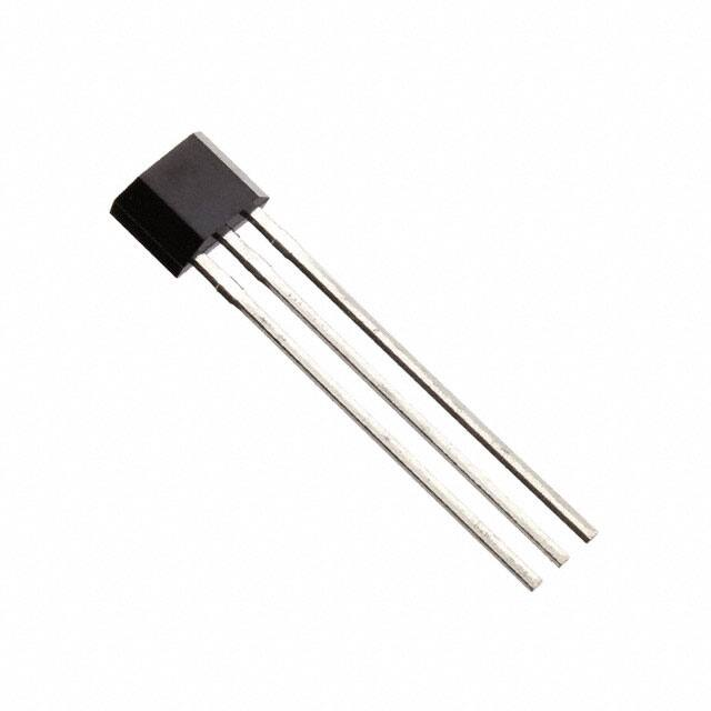
TO-92S
Pin Definition:
1. VDD
2. GND
3. Output
Description
TSH181, Hall-Effect sensor, designed for electronic commutation of brush-less DC motor applications. The
device includes an on-chip Hall voltage generator for magnetic sensing, a comparator that amplifies the Hall
Voltage, and a Schmitt trigger to provide switching hysteresis for noise rejection, and open collector output. An
internal band gap regulator is used to provide temperature compensated supply voltage for internal circuits and
allows a wide operating supply range. The device is identical except for magnetic switch points. The device
includes on a single silicon chip a voltage regulator, Hall-voltage generator, small-signal amplifier, chopper
stabilization, Schmitt trigger, open-collector output to sink up to 25mA. A south pole of sufficient strength will turn
the output on. The North Pole is necessary to turn the output off. An on-board regulator permits operation with
supply voltages of 3.5V to 20 V.
Features
●
●
●
●
●
Temperature compensation.
Wide operating voltage range.
Open-Collector pre-driver.
Reverse bias protection on power supply pin.
o
100% at 125 C “Hot Test”
Ordering Information
Part No.
TSH181CT B0G
Package
Packing
TO-92S
1Kpcs / Bulk Bag
Note: “G” denote for Halogen Free Product
Application
●
●
●
●
●
High temperature Fan motor
3 phase BLDC motor application
Fan motor application
Speed sensing
Revolution counting
Absolute Maximum Rating (Ta = 25oC unless otherwise noted)
Characteristics
Limit
Value
Unit
Supply voltage
VCC
20
V
Output Voltage
VOUT
30
V
Reverse voltage
VCC/OUT
-20
V
Unlimited
Gauss
mA
Magnetic flux density
Output current
IOUT
25
Operating Temperature Range
TOPR
-40 to +125
Storage temperature range
TSTG
o
C
o
C
-55 to +150
o
Maximum Junction Temp
TJ
150
C
Thermal Resistance - Junction to Ambient
θJA
206
o
Thermal Resistance - Junction to Case
θJC
148
o
Package Power Dissipation
PD
606
C/W
C/W
mW
Note: Do not apply reverse voltage to VCC and VOUT Pin, It may be caused for Miss function or damaged device.
1/7
Version: B13
�TSH181
General Purpose Hall Effect Latch
Block Diagram
Typical Application Circuit
C1:1000pF
C2:15pF
R1:10KΩ
Electrical Specifications (DC Operating Parameters:TA=+25oC,VCC=12V)
Parameters
Test Conditions
Min
Typ
Max
Units
3.5
--
20
V
Supply Voltage
Operating
Supply Current
B< BOP
--
4
8
mA
Output Saturation Voltage
IOUT = 10mA, B>BOP
--
--
700
mV
Output Leakage Current
IOFF BBOP
Open
South pole
Low
B
很抱歉,暂时无法提供与“TSH181CT B0G”相匹配的价格&库存,您可以联系我们找货
免费人工找货- 国内价格
- 1+3.89880
- 200+1.55520
- 500+1.50120
- 1000+1.47960
- 国内价格 香港价格
- 1+9.149591+1.18596