SM2305
P-Channel Enhancement-Mode MOSFET (-20V, -4. 5A)
PRODUCT SUMMARY
VDSS
ID
-20V
-4.5A
RDS(on) (m-ohm) Max
53 @ VGS = -10V,ID=-4.5A
60 @ VGS = -4.5V,ID=-4.2A
100 @ VGS = -2.5V,ID=-2.0A
◆ Features
1、Super high dense cell trench design for low RDS(on).
2、Rugged and reliable.
3、SOT-23 package
4、RoHS Compliant.
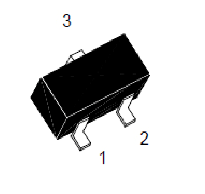
SM2305 Pin Assignment & Symbol
◆ Ordering Information
Ordering Number
Lead Free
Halogen Free
SM2305SRL
SM2305LRL
SM2305SRG
SM2305LRG
(2)Packing Type
1
G
G
SOT-23
SOT-23-3L
SM2305X X X
(1)Package Type
Pin Assignment
Package
3
D
D
Packing
Tape Reel
Tape Reel
(1) S:SOT-23;L:SOT-23-3L
(2) R:Tape Reel
(3) G:Halogen Free;L:Lead Free
(3)Lead Free
V01
2
S
S
1
www.sourcechips.com
�SM2305
◆ Absolute Maximum Ratings (TA=25oC, unless otherwise noted)
Symbol
Parameter
Ratings
Units
VDS
Drain-Source Voltage
-20
V
VGS
Gate-Source Voltage
Maximum Power Dissipation @TA=25
±12
V
PD
℃
Maximum Power Dissipation t @TA=70℃
Drain Current (Pulsed)
ID
Continuous Drain Current @TA=25
RqJA
W
0.7
*1
IDM
Tj, Tstg
1.1
-20
A
-4.5
A
-55 to +150
°C
110
°C/W
℃
Operating Junction and Storage Temperature Range
Thermal Resistance Junction to Ambient
a: Surface Mounted on FR4 Board , t ≤ 5sec .
b: 1 Pulse Test: Pulse width ≤ 300us , Duty Cycle ≤ 2% .
◆ Electrical Characteristics (TA=25°C, unless otherwise noted)
Symbol
Characteristic
Test Conditions
Min.
Typ.
Max.
Unit
● Off Characteristics
BVDSS
Drain-Source Breakdown Voltage
VGS=0V, ID=-250uA
IDSS
Zero Gate Voltage Drain Current
IGSS
Gate-Body Leakage Current
● On Characteristics
VGS(th)
RDS(on)
gfs
-20
-
-
VDS=-20V, VGS=0V
o
VDS=-16V, VGS=0V, TJ=55 C
-
-
-1
-
-
-10
VGS=±12V, VDS=0V
-
-
±100
VDS=VGS, ID=-250uA
-0.6
-0.85
-1.4
VGS=-10V, ID=-4.5A
-
-
53
VGS=-4.5V, ID=-4.2A
-
-
60
VGS=-2.5V, ID=-2.0A
-
-
100
VDS=-5V, ID=-4.7A
-
14
-
-
920
-
-
90
-
-
85
-
-
4.5
-
-
24
18
2.7
22
35
45
25
27
14
31.2
23.4
3.51
44
70
90
50
-
-
-
V
uA
nA
c
Gate Threshold Voltage
Drain-Source On-State Resistance
Forward Transconductance
● Dynamic Characteristics
Ciss
Input Capacitance
Output Capacitance
Crss
Reverse Transfer Capacitance
Rg
Gate Resistance
● Switching Characteristics
Total Gate Charge
Qgs
Gate-Source Charge
Qgd
Gate-Drain Charge
td(on)
Turn-on Delay Time
tr
Turn-on Rise Time
td(off)
Turn-off Delay Time
mΩ
S
d
Coss
Qg
V
VDS=-20V, VGS=0V, f=1MHz
VDS=0V, VGS=0V, f=1MHz
pF
Ω
d
tf
Turn-off Fall Time
trr
Reverse Recovery Time
Qrr
Reverse Recovery Charge
VDS=-10V, ID=-4.7A, VGS=-4.5V
VDD=-10V, RD=10Ω, ID=-1A,
VGS=-4.5V, RG=6Ω
IDS=-4A, dI/ dt=100A/ uS
nC
nS
nS
nC
● Drain-Source Diode Characteristics
VSD
VGS=0V, IS=-1.7A
Drain-Source Diode Forward Voltage
b:Pulse Test: Pulse Width £300us, Duty Cycle£2%
c: Guaranteed by design , not subject to production testing.
V01
2
www.sourcechips.com
-1.2
V
�SM2305
◆ Characteristics Curve
V01
3
www.sourcechips.com
�SM2305
◆ Characteristics Curve
V01
4
www.sourcechips.com
�SM2305
◆ Characteristics Curve
V01
5
www.sourcechips.com
�
很抱歉,暂时无法提供与“SM2305SRL”相匹配的价格&库存,您可以联系我们找货
免费人工找货- 国内价格
- 1+0.28476
- 100+0.26578
- 300+0.24679
- 500+0.22781
- 2000+0.21832
- 5000+0.21262