IRFZ44N-B
N-Channel MOSFET
Features:
Low Intrinsic Capacitances.
Excellent Switching Characteristics.
Extended Safe Operating Area.
Unrivalled Gate Charge :Qg= 31nC (Typ.).
BVDSS=60V,ID=50A
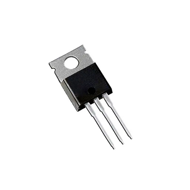
TO-220
r
RDS(on) : 22mΩ (Max) @VG=10V
to
100% Avalanche Tested
1.Gate
(G)
2.Drain (D)
3.Source (S)
Absolute Maximum Ratings*
co
nd
uc
□
□
□
□
□
□
□
(Tc=25℃ unless otherwise noted)
Parameter
VDSS
Drain-Source Voltage
Se
mi
Symbol
IAR
PD
Tstg
TL
V
50
TC=100℃
35.4
A
Gate Threshold Voltage
±25
V
Single Pulse Avalanche Energy (note1)
490
mJ
Avalanche Current (note2)
50
A
Power Dissipation (Tc=25℃)
120
W
Junction Temperature(MAX)
150
Storage Temperature
Maximum lead temperature for soldering purpose,1/8” from
case for 5 seconds
-55~+150
JS
MI
Tj
60
TC=25℃
CR
O
EAS
Unit
Drain Current
ID
VGSS
Value
℃
300
Thermal Characteristics
Symbol
Parameter
Typ.
MAX.
RθJC
Thermal Resistance,Junction to Case
-
1.24
RθJA
Thermal Resistance,Junction to Ambient
-
62.5
RθCS
Thermal Resistance,Case to Sink
-
0.5
www.jsmsemi.com
Unit
℃/W
第1/7页
�IRFZ44N-B
N-Channel MOSFET
Electrical Characteristics Tc=25℃ unless other wise noted
Symbol
Parameter
Test Condition
Min.
Typ.
Max
Units
--
--
V
Off Characteristics
Drain-Sourse Breakdown Voltage
ID=250μA,VGS=0
△BVDSS/
△TJ
Breakdown Voltage Temperature
Conficient
ID=250μA,Reference to
25℃
--
0.06
--
V/℃
IDSS
Zero Gate Voltage Drain Current
Vds=60V, Vgs=0V
--
--
1
μA
10
μA
r
60
BVDSS
100
nA
--
-100
nA
2
--
4
V
--
--
0.022
Ω
--
1180
1540
pF
--
440
580
pF
--
65
90
pF
--
15
40
nS
--
105
220
nS
60
130
nS
--
65
140
nS
--
31
41
nC
--
8
--
IGSSR
Gate-body leakage
Current,Reverse
Vgs=+25V, Vds=0V
--
Vgs=-25V, Vds=0V
On Characteristics
Date Threshold Voltage
Id=250uA,Vds=Vgs
RDS(on)
Static Drain-Sourse
On-Resistance
Id=25A,Vgs=10V
--
co
nd
VGS(th)
--
to
Gate-body leakage
Current,Forward
uc
IGSSF
Vds=48V, Tc=125 ℃
Input Capacitance
Coss
Output Capacitance
Crss
Reverse Transfer Capacitance
VDS=25V,VGS=0,
f=1.0MHz
Se
Ciss
mi
Dynamic Characteristics
CR
O
Switching Characteristics
Td(on)
Turn-On Delay Time
Tr
Turn-On Rise Time
Td(off)
Turn-Off Delay Time
Turn-Off Fall Time
Qg
Total Gate Charge
JS
MI
Tf
Qgs
Gate-Sourse Charge
Qgd
Gate-Drain Charge
VDD=250V,ID=25A
RG=25Ω (Note 3,4)
VDS=400,VGS=10V,
ID=25A (Note 3,4)
--
nC
13
--
nC
--
50
A
200
A
Drain-Sourse Diode Characteristics and Maximum Ratings
IS
Maximun Continuous Drain-Sourse Diode Forward Current
ISM
Maximun Plused Drain-Sourse DiodeForwad Current
VSD
Drain-Sourse Diode Forward
Voltage
trr
Qrr
*Notes
Reverse Recovery Time
Reverse Recovery Charge
---
--
Id=25A
--
--
1.5
V
IS=25A,VGS =0V
diF/dt=100A/μs (Note3)
--
52
--
nS
75
--
μC
--
1, L=9.3mH, IAS=50A, VDD=50V, RG=25Ω, Starting TJ =25°C
2, Repetitive Rating : Pulse width limited by maximum junction temperature
3, Pulse Test : Pulse Width ≤ 300μs, Duty Cycle ≤ 2%
4, Essentially Independent of Operating Temperature
www.jsmsemi.com
第2/7页
�IRFZ44N-B
N-Channel MOSFET
Typical Characteristics
VGS
15.0 V
10.0 V
8.0 V
7.0 V
6.0 V
5.5 V
5.0 V
Bottom : 4.5 V
Top :
1
10
1
10
r
ID, Drain Current [A]
2
10
ID, Drain Current [A]
2
10
175℃
0
to
25℃
※ Note :
1. 250μ s Pulse Test
2. TC = 25℃
※ Notes :
1. VDS = 30V
2. 250μ s Pulse Test
-55℃
10
0
0
10
1
10
2
10
4
Figure 2. Transfer Characteristics
0.05
2
co
VGS = 10V
mi
VGS = 20V
IDR, Reverse Drain Current [A]
0.04
1
10
0.02
0.01
Se
R DS(ON) [ Ω ],
10
Drain-Source On-Resistance
10
nd
Figure 1. On-Region Characteristics
※ Note : TJ = 25℃
0.00
0
50
100
150
200
0
CR
O
0.2
10
Ciss
※ Notes :
1. VGS = 0 V
2. f = 1 MHz
1500
1000
Crss
500
V GS , Gate-Source Voltage [V]
Coss
0.8
1.0
1.2
1.4
1.6
12
Ciss = Cgs + Cgd (Cds = shorted)
Coss = Cds + Cgd
Crss = Cgd
JS
MI
0.6
Figure 4. Body Diode Forward Voltage
Variation vs. Source Current
and Temperature
2500
2000
0.4
VSD, Source-Drain voltage [V]
Figure 3. On-Resistance Variation vs.
Drain Current and Gate Voltage
3000
※ Notes :
1. VGS = 0V
2. 250μ s Pulse Test
25℃
175℃
10
ID, Drain Current [A]
Capacitance [pF]
8
VGS, Gate-Source Voltage [V]
VDS, Drain-Source Voltage [V]
0.03
6
uc
-1
10
VDS = 30V
VDS = 48V
8
6
4
2
※ Note : ID = 50A
0
0
-1
10
0
0
10
5
10
15
20
25
30
35
1
10
QG, Total Gate Charge [nC]
VDS, Drain-Source Voltage [V]
Figure 5. Capacitance Characteristics
Figure 6. Gate Charge Characteristics
www.jsmsemi.com
第3/7页
�IRFZ44N-B
N-Channel MOSFET
Typical Characteristics
(Continued)
2.5
2.0
1.1
RDS(ON) , (Normalized)
Drain-Source On-Resistance
1.5
1.0
0.8
-100
-50
0
50
100
0.5
150
※ Notes :
1. VGS = 10 V
2. ID = 25 A
0.0
-100
200
-50
150
200
Figure 8. On-Resistance Variation
vs. Temperature
3
60
co
Operation in This Area
is Limited by R DS(on)
100μ s
2
mi
1 ms
10 ms
DC
1
※ Notes :
o
1. TC = 25 C
o
2. TJ = 175 C
3. Single Pulse
0
10
-1
10
0
1
10
10
40
30
20
10
0
25
2
CR
O
10
ID , Drain Current [A]
50
Se
ID , Drain Current [A]
100
nd
Figure 7. Breakdown Voltage Variation
vs. Temperature
10
50
TJ, Junction Temperature [ C]
TJ, Junction Temperature [ C]
10
0
o
o
10
to
0.9
r
1.0
※ Notes :
1. VGS = 0 V
2. ID = 250 μ A
uc
BV DSS , (Normalized)
Drain-Source Breakdown Voltage
1.2
50
VDS, Drain-Source Voltage [V]
100
125
150
175
Figure 10. Maximum Drain Current
vs. Case Temperature
0
D = 0 .5
※ N otes :
1 . Z θ J C( t ) = 1 . 2 4 ℃ /W M a x .
2 . D u t y F a c t o r , D = t 1 /t 2
3 . T J M - T C = P D M * Z θ J C( t )
0 .2
0 .1
10
-1
0 .0 5
PDM
0 .0 2
JC
JS
MI
(t), T h e rm a l R e s p o n s e
Figure 9. Maximum Safe Operating Area
10
75
TC, Case Temperature [℃]
t1
0 .0 1
t2
Z
θ
s in g le p u ls e
10
-2
10
-5
10
-4
10
-3
10
-2
10
-1
10
0
10
1
t1 , S q u a r e W a v e P u ls e D u r a tio n [s e c ]
Figure 11. Transient Thermal Response Curve
www.jsmsemi.com
第4/7页
�IRFZ44N-B
N-Channel MOSFET
Typical Characteristics
(Continued)
Gate Charge Test Circuit & Waveform
to
Qg
10V
300nF
VDS
VGS
Qgs
nd
DUT
Qgd
uc
50KΩ
200nF
12V
r
VGS
Same Type
as DUT
co
3mA
Charge
RL
Se
VDS
mi
Resistive Switching Test Circuit & Waveforms
CR
O
JS
MI
10%
VGS
DUT
td(on)
tr
td(off)
t on
tf
t off
Unclamped Inductive Switching Test Circuit & Waveforms
BVDSS
1
EAS = ---- L IAS2 -------------------2
BVDSS - VDD
L
VDS
BVDSS
IAS
ID
RG
VDD
DUT
10V
90%
VDD
VGS
RG
10V
VDS
ID (t)
VDS (t)
VDD
tp
tp
www.jsmsemi.com
Time
第5/7页
�IRFZ44N-B
N-Channel MOSFET
Typical Characteristics
(Continued)
or
Peak Diode Recovery dv/dt Test Circuit & Waveforms
+
DUT
ct
VDS
I SD
Driver
RG
ic
Same Type
as DUT
on
L
du
_
VGS
VDD
MI
CR
O
VGS
( Driver )
S
em
• dv/dt controlled by RG
• ISD controlled by pulse period
Gate Pulse Width
D = -------------------------Gate Pulse Period
10V
IFM , Body Diode Forward Current
JS
I SD
( DUT )
di/dt
IRM
Body Diode Reverse Current
VDS
( DUT )
Body Diode Recovery dv/dt
VSD
VDD
Body Diode
Forward Voltage Drop
www.jsmsemi.com
第6/7页
�IRFZ44N-B
N-Channel MOSFET
TO-220AB
JS
MI
CR
O
Se
mi
co
nd
uc
to
r
Unit: mm
Symbol
W
W1
W2
W3
*
W4
Size
Min
Max
9.66
10.28
2.54(TYP)
0.70
0.95
1.17
1.37
1.32
1.72
Symbol
W5
L
L1
L2
L3
Size
Min
9.80
9.00
6.40
2.70
12.70
Max
10.20
9.40
6.80
2.90
14.27
Symbol
L4**
L5
T
T1
T2
www.jsmsemi.com
Size
Min
6.20
2.79
4.30
1.15
2.20
Max
6.60
3.30
4.70
1.40
2.60
Symbol
T3
G(Φ)
Size
Min
0.45
3.50
Max
0.60
3.70
第7/7页
�