UDD32CXXL01 SERIES
Electrostatic Discharged Protection Devices (ESD) Data Sheet
Description
The series are an ultra low capacitance TVS array designed to protect
high speed data interfaces. This series has been specifically designed
to protect sensitive components which are connected to data an trans-mission lines from overvoltage caused by electrostatic discharge (ESD),
cable discharge events (CDE) and lightning.
The unique design incorporates surge rated, low capacitance steering
diodes and a TVS diode in a single package. During transient conditions,
the steering diodes direct the transient current to ground. The internal
TVS diode clamps the transient voltage to a safe level. The ultra low
capacitance array configuration allows the user to protect up to the high
speed data lines. These devices are in a signal package, RoHS/WEEE
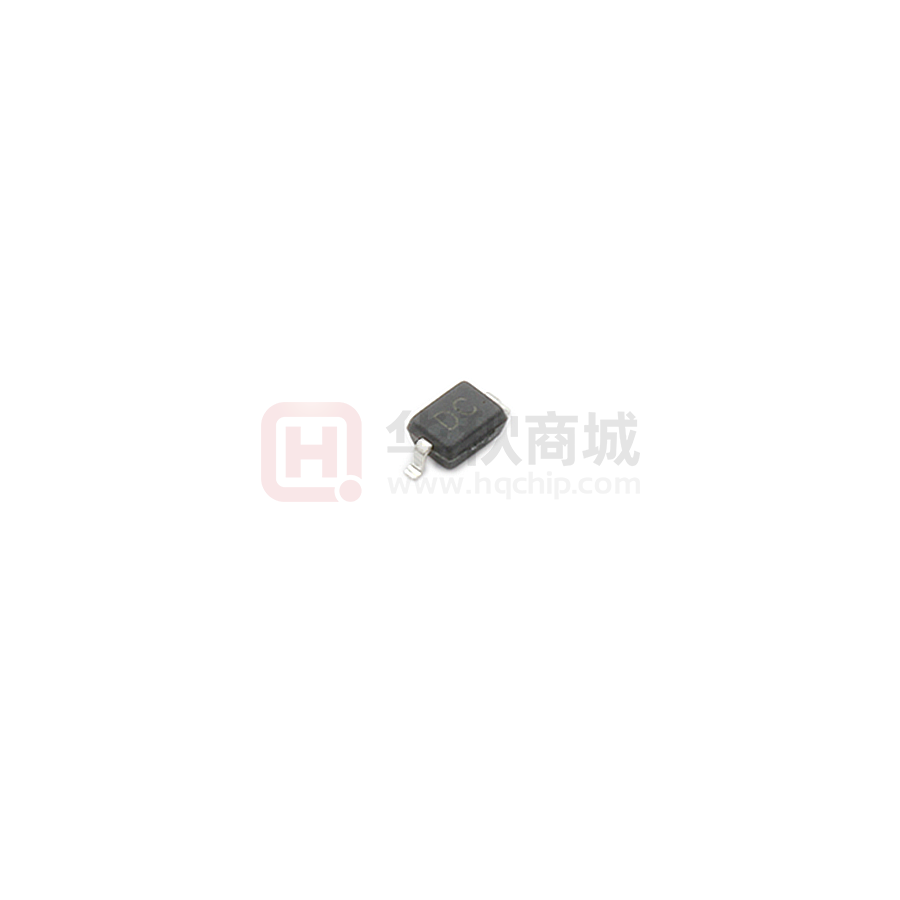
compliant, SOD-323 package. It measures 2.5×1.25×1.0mm.
The series devices may be used to meet the immunity requirements of
IEC61000-4-2 (ESD), IEC61000-4-4 (EFT) and IEC61000-4-5 (Surge).
Features
● IEC61000-4-2 ESD 30KV Air, 30KV contact compliance
●
●
●
●
●
●
●
●
●
●
ESD 15KV Air, 8KV contact compliance for UDD32C36L01
SOD-323 surface mount package
Protects one I/O line
Working voltage: 3V, 5V, 8V, 12V ,15V, 24V, 36V
Low leakage current
Low operating and clamping voltages
Solid-state silicon avalanche technology
Lead Free/RoHS compliant
Solder reflow temperature: Pure Tin-Sn, 260~270℃
Flammability rating UL 94V-0
Meets MSL level 1, per J-STD-020
Pin Configuration
Applications
●
●
●
●
●
USB 2.0 and USB 3.0 interface
10/100/1000 Ethernet
Personal digital assistants (PDA)
Serial ATA protection
Digital visual interface (DVI)
Revision:ESD-UDD32CXXL01 SERIES-001(A2)
●
●
●
●
Wireless system devices
Handhelds and notebooks
Digital cameras
RF interface
1/6
http://brightking.yageo.com
�UDD32CXXL01 SERIES
Maximum Ratings
Rating
Symbol
Value
Unit
PPP
350
W
Peak pulse power (tp=8/20μs waveform)
ESD voltage (Contact discharge)
±30
VESD
kV
ESD voltage (Air discharge)
±30
Storage & operating temperature range
TSTG ,TJ
℃
-55~+150
Electrical Characteristics (TJ=25℃)
UDD32C03L01 (Marking: AC)
Parameter
Reverse stand-off voltage
Reverse breakdown voltage
Symbol
Condition
Min.
Typ.
VRWM
Max.
Unit
3.3
V
VBR
IBR=1mA
4
V
Reverse leakage current
IR
VR=3.3V
5
μA
Clamping voltage (tp=8/20μs)
VC
IPP=1A
7
V
Clamping voltage (tp=8/20μs)
VC
IPP=5A
15
V
Peak Pulse Current (tp=8/20μs)
IPP
19
A
Off state junction capacitance
CJ
0Vdc,f=1MHz
Symbol
Condition
0.8
pF
UDD32C05L01 (Marking: BC)
Parameter
Reverse stand-off voltage
Reverse breakdown voltage
Min.
Typ.
VRWM
Max.
Unit
5
V
VBR
IBR=1mA
6
V
Reverse leakage current
IR
VR=5V
5
μA
Clamping voltage (tp=8/20μs)
VC
IPP=1A
9.8
V
Clamping voltage (tp=8/20μs)
VC
IPP=5A
18.3
V
Peak Pulse Current (tp=8/20μs)
IPP
17
A
Off state junction capacitance
CJ
0Vdc,f=1MHz
Symbol
Condition
0.8
pF
UDD32C08L01(Marking: BC.)
Parameter
Reverse stand-off voltage
Reverse breakdown voltage
Min.
Typ.
VRWM
Max.
Unit
8
V
VBR
IBR=1mA
Reverse leakage current
IR
VR=8V
1
μA
Clamping voltage (tp=8/20μs)
VC
IPP=1A
13
V
Clamping voltage (tp=8/20μs)
VC
IPP=10A
24
V
Peak Pulse Current (tp=8/20μs)
IPP
17
A
Off state junction capacitance
CJ
Revision:ESD-UDD32CXXL01 SERIES-001(A2)
0Vdc,f=1MHz
2/6
8.5
V
1
pF
http://brightking.yageo.com
�UDD32CXXL01 SERIES
UDD32C12L01 (Marking: DC)
Parameter
Reverse stand-off voltage
Reverse breakdown voltage
Symbol
Condition
Min.
Typ.
VRWM
Max.
Unit
12
V
VBR
IBR=1mA
13.3
V
Reverse leakage current
IR
VR=12V
1
μA
Clamping voltage (tp=8/20μs)
VC
IPP=1A
19
V
Clamping voltage (tp=8/20μs)
VC
IPP=5A
28.6
V
Peak Pulse Current (tp=8/20μs)
IPP
7
A
Off state junction capacitance
CJ
0Vdc,f=1MHz
Symbol
Condition
0.8
pF
UDD32C15L01 (Marking: EC)
Parameter
Reverse stand-off voltage
Reverse breakdown voltage
Min.
Typ.
VRWM
Max.
Unit
15
V
VBR
IBR=1mA
16.7
V
Reverse leakage current
IR
VR=15V
1
μA
Clamping voltage (tp=8/20μs)
VC
IPP=1A
24
V
Clamping voltage (tp=8/20μs)
VC
IPP=5A
35
V
Peak Pulse Current (tp=8/20μs)
IPP
6
A
Off state junction capacitance
CJ
0Vdc,f=1MHz
Symbol
Condition
0.8
pF
UDD32C24L01 (Marking: HC)
Parameter
Reverse stand-off voltage
Reverse breakdown voltage
Min.
Typ.
VRWM
Max.
Unit
24
V
VBR
IBR=1mA
Reverse leakage current
IR
VR=24V
1
μA
Clamping voltage (tp=8/20μs)
VC
IPP=1A
43
V
Clamping voltage (tp=8/20μs)
VC
IPP=5A
56
V
Peak Pulse Current (tp=8/20μs)
IPP
6
A
Off state junction capacitance
CJ
Revision:ESD-UDD32CXXL01 SERIES-001(A2)
0Vdc,f=1MHz
3/6
26.7
V
0.8
pF
http://brightking.yageo.com
�UDD32CXXL01 SERIES
UDD32C36L01 (Marking: KC)
Parameter
Symbol
Reverse stand-off voltage
Condition
Min.
Typ.
VRWM
Reverse breakdown voltage
Max.
Unit
36
V
VBR
IBR=1mA
40
V
Reverse leakage current
IR
VR=36V
1
μA
Clamping voltage (tp=8/20μs)
VC
IPP=1A
70
V
Clamping voltage (tp=8/20μs)
VC
IPP=2A
75
V
Peak Pulse Current (tp=8/20μs)
IPP
3
A
Off state junction capacitance
CJ
0Vdc,f=1MHz
0.8
pF
Typical Characteristics Curves
Figure 1. Power Derating Curve
Figure 2. Pulse Waveform
110
100
90
% of Peak Power Current
Peak Power Dissipation (%)
100
80
70
60
50
40
30
20
10
0
tr
Peak value Ipp
Waveform
Parameters:
tr=8µs
td=20µs
90
80
70
60
50
40
td=t|PP/2
30
20
10
0
25
50
75
100
125
150
175
0
200
0
5
10
15
20
25
30
t-Time (μs)
TA-Ambient Temperature (℃)
Figure 3. Non-Repetitive Peak Pulse vs Pulse Time
Figure 4. ESD Clamping (8kV Contact IEC61000-4-2)
PPP-Peak Pusle Power (W)
10000
1000
100
10
0.1
1
10
100
1000
10000
tp-Pulse Duration (μs)
Revision:ESD-UDD32CXXL01 SERIES-001(A2)
4/6
http://brightking.yageo.com
�UDD32CXXL01 SERIES
Recommended Soldering Conditions
Reflow Soldering
Critical Zone
TL to TP
tP
TP
Ramp-up
TL
tL
Temperature
TS max
TS min
Ramp-down
tS
Preheat
25
t 25℃ to Peak
Time
Recommended Condition
Profile Feature
Pb-Free Assembly
Average ramp-up rate (TL to TP)
3℃/second max.
Preheat
-Temperature Min (TS min)
-Temperature Max (TS max)
-Time (min to max) (ts)
150℃
200℃
60-180 seconds
TS max to TL
-Ramp-up Rate
3℃/second max.
Time maintained above:
-Temperature (TL)
-Time (tL)
217℃
60-150 seconds
Peak Temperature (TP)
260℃
Time within 5℃ of actual Peak Temperature (tP)
20-40 seconds
Ramp-down Rate
6℃/second max.
Time 25℃ to Peak Temperature
Revision:ESD-UDD32CXXL01 SERIES-001(A2)
8 minutes max.
5/6
http://brightking.yageo.com
�UDD32CXXL01 SERIES
Dimensions (SOD-323)
G
E
Dimension
Symbol
Millimeters
X
H
1
2
A
F
D
B
C
detail X
0.50
(2X)
0.60
(2X)
2.3
Recommended Soldering Pad Layout
Inches
Min.
Max.
Min.
Max.
A
0.80
1.10
0.031
0.043
B
0.00
0.10
0.000
0.004
C
0.20
-
0.008
-
D
0.11
0.20
0.004
0.008
E
1.15
1.35
0.045
0.053
F
0.25
0.35
0.010
0.014
G
1.60
1.80
0.063
0.071
H
2.40
2.70
0.094
0.102
Packaging
Tape
P0
P2
K
F
B0
B
W
E
øD0
P1
A0
øD1
t
A
Symbol
Dimension (mm)
W
8.00±0.30
P0
4.00±0.10
P1
4.00±0.10
P2
2.00±0.10
D0
Φ1.55±0.10
D1
Φ1.00±0.05
E
1.75±0.10
F
3.50±0.10
A
1.48±0.10
A0
0.80±0.10
B
3.00±0.10
B0
1.80±0.10
K
1.05±0.10
t
0.25±0.05
D
Φ178.0±2.0
D2
Φ13.0
W1
9.5
Reel
D2
D
Revision:ESD-UDD32CXXL01 SERIES-001(A2)
W1
Quantity: 3000PCS
6/6
http://brightking.yageo.com
�
很抱歉,暂时无法提供与“UDD32C12L01”相匹配的价格&库存,您可以联系我们找货
免费人工找货- 国内价格
- 10+0.40996
- 100+0.32819
- 600+0.28730
- 1200+0.28299
- 3000+0.23582
- 30000+0.23346
- 国内价格
- 10+0.44723
- 100+0.35802
- 300+0.31342
- 3000+0.25726
- 国内价格
- 1+0.40480
- 200+0.26070
- 1500+0.22770
- 3000+0.20130
- 国内价格
- 10+0.45360
- 100+0.37800
- 300+0.33480
- 3000+0.29160
- 6000+0.27000
- 9000+0.25920
- 国内价格
- 150+0.23760
- 500+0.22220
- 国内价格
- 20+0.81940
- 100+0.48870
- 800+0.34210
- 3000+0.24440
- 6000+0.23220
- 30000+0.21500