SL2308
60V N-Channel Enhancement Mode MOSFET
DESCRIPTION
FEATURE
high cell density advanced trench technology..
60V/1 . 8 A, R DS(ON) =1 35mΩ(typ.)@VGS=1 0V
60V/ 1 ..5 A, R DS(ON)=1 54m Ω (typ.)@VGS=4.5V
Super high design for extremely low RDS(ON)
This high density process is especially tailored to
The SL2308 is the N-Channel logic enhancement
Exceptional on-resistance and Maximum DC
S Un
em i
ve
C
on co r
C
fi nd h
de u ip
c
nt t
o
ia r
l
mode power field effect transistor is produced using
current capability
minimize on-state resistance. These devices are
particularly suited for low voltage application, and
This is a Full RoHS compliance
low in-line power loss are needed in a very small
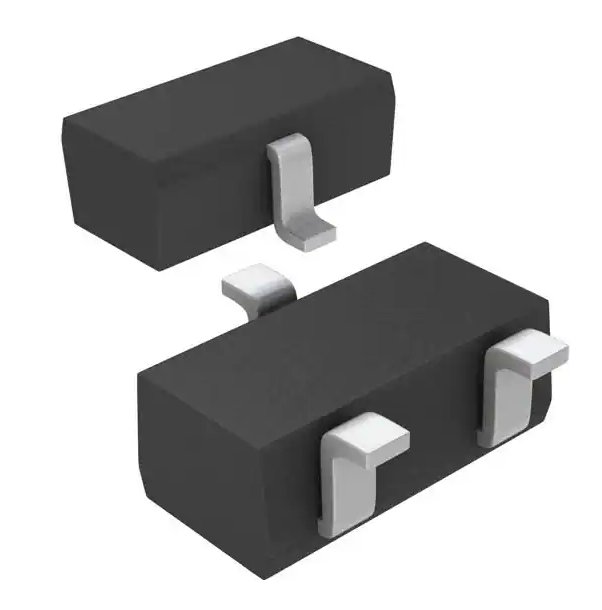
SOT23-3 package design
outline surface mount package.
APPLICATIONS
PIN CONFIGURATION
www.slkormicro.com
1
Power Management in Note Book
Portable Equipment
Battery Powered System
�SL2308
ABSOLUTE MAXIMUM RATINGS ( TA = 25℃
Symbol
Unless otherwise noted )
Parameter
Typical
Unit
VDSS
Drain-Source Voltage
60
V
VGSS
Gate-Source Voltage
±20
V
1.8
A
Continuous Drain Current (TJ=150℃)
VGS-4.5V
IDM
Pulsed Drain Current
10
A
IS
Continuous Source Current (Diode Conduction)
1
A
PD
Power Dissipation
TJ
Operation Junction Temperature
U
em ni
ve
co r
C
nd h
i
uc p
to
r
ID
TSTG
TA=25℃
1.25
TA=75℃
0.8
Storage Temperature Range
W
150
℃
-55~+150
℃
Note: Absolute maximum ratings are those values beyond which the device could be permanently damaged.
Absolute maximum ratings are stress rating only and functional device operation is not implied
THERMAL DATA
Symbol
Min
Thermal Resistance-Junction to Ambient
S
RθJA
Parameter
www.slkormicro.com
2
Typ
Max
Unit
62.5
125
℃/W
�SL2308
ELECTRICAL CHARACTERISTICS(VDD=2.75V, TA=25℃
Symbol
Parameter
Condition
Unless otherwise noted)
Min
Typ
Max
Unit
Static Parameters
V(BR)DSS
Drain-Source Breakdown Voltage
VGS=0V, ID=250uA
60
VGS(th)
Gate Threshold Voltage
VDS=VGS, ID=250uA
1.0
IGSS
Gate Leakage Current
IDSS
V
2
V
VDS=0V, VGS=±12V
±100
nA
VDS=44V, VGS=0
1
VDS=44V, VGS=0
Zero Gate Voltage Drain Current
5
S
e
C m
on c
o
fi n
de d
u
nt c
ia to
l r
TJ=85℃
uA
ID(ON)
RDS(ON)
Gfs
On=State Drain Current
VDS≧5V, VGS=4.5V
Drain-Source On-Resistance
10
A
VGS =10V,I D=1.8A
135
160
VGS=4.5V, ID=1.5A
154
200
mΩ
Forward Transconductance
VDS=5V, ID=2.1A
10
IS=1.0A, VGS=0V
0.8
1.0
3.9
S
Source-Drain Diode
VSD
Diode Forward Voltage
V
Dynamic Parameters
Qg
Total Gate Charge
VDS=27V
2.1
Qgs
Gate-Source Charge
VGS=4.5V
0.6
Qgd
Gate-Drain Charge
ID=2.1A
0.8
Ciss
Input Capacitance
VDS=25V
295
Coss
Output Capacitance
VGS=0V
40
Crss
Reverse Transfer Capacitance
f=1MHz
15
VDS=27V
3.6
RL=10Ω
3.5
ID=1A
32
Td(on)
Tr
Turn-On Time
Td(off)
Tf
VGEN=4.5V
Turn-Off Time
RG=6Ω
3
Note: 1. Pulse test: pulse width
很抱歉,暂时无法提供与“SL2308”相匹配的价格&库存,您可以联系我们找货
免费人工找货- 国内价格
- 1+0.19040
- 30+0.18360
- 100+0.17680
- 500+0.16320
- 1000+0.15640
- 2000+0.15232
