FDMA905P
P-Channel Enhancement Mode Power MOSFET
Description
D
The FDMA905P uses advanced trench technology to
provide excellent RDS(ON), low gate charge and operation
G
with gate
voltages .This device is suitable for use as a load switching
application and a wide variety of other applications.
S
to
r
General Features
Schematic diagram
● VDS = -12V,ID =-16A
RDS(ON) < 22mΩ @ VGS=-2.5V
uc
RDS(ON) < 18mΩ @ VGS=-4.5V
● Advanced trench MOSFET process technology
nd
● Ultra low on-resistance with low gate charge
Pin assignment
co
Application
●PWM applications
●Load switch
Se
mi
●Battery charge in cellular handset
DFN2X2-6L bottom view
Device Marking
Device
FDMA905P
Device Package
Reel Size
Tape Width
Quantity
DFN2X2-6L
-
-
-
JS
MI
905T
CR
O
Package marking and ordering information
Absolute maximum ratings (TA=25℃unless otherwise noted)
Parameter
Symbol
Drain-Source Voltage
VDS
Gate-Source Voltage
VGS
Drain Current-Continuous
ID
Drain Current -Pulsed (Note 1)
IDM
Maximum Power Dissipation
PD
Operating Junction and Storage Temperature Range
TJ,TSTG
Limit
Unit
-12
V
±8
V
-16
A
-65
A
2.5
W
-55 To 150
℃
Thermal Characteristic
Thermal Resistance,Junction-to-Ambient (Note 2)
RθJA
50
℃/W
Thermal Resistance,Junction-to-Case (Note 2)
RθJC
6.9
℃/W
www.jsmsemi.com
第1/5页
�FDMA905P
P-Channel Enhancement Mode Power MOSFET
Electrical characteristics (TA=25℃unless otherwise noted)
Parameter
Symbol
Condition
Min
Typ
Max
Unit
Drain-Source Breakdown Voltage
V(BR) DSS
VGS=0V ID=-250μA
-12
-
-
V
Zero Gate Voltage Drain Current
IDSS
VDS=-12V,VGS=0V
-
-
-1
μA
Gate-Body Leakage Current
IGSS
VGS=±8V,VDS=0V
-
-
±100
nA
Gate Threshold Voltage
VGS(th)
VDS=VGS,ID=-250μA
-0.4
-0.7
-1
V
Drain-Source On-State Resistance
RDS(ON)
VGS=-4.5V, ID=-6.7A
-
12
18
mΩ
-
14
22
mΩ
-
40
-
S
-
2700
-
PF
-
680
-
PF
-
590
-
PF
-
11
-
nS
VDD=-10V,ID=-1A
-
35
-
nS
VGS=-4.5V,RGEN=10Ω
-
30
-
nS
-
10
-
nS
-
35
48
nC
-
5
-
nC
-
10
-
nC
-
-
-1.2
V
-
-
-16
A
On Characteristics (Note 3)
gFS
VDS=-10V,ID=-6.7A
uc
Forward Transconductance
VGS=-2.5V, ID=-6.2A
Dynamic Characteristics (Note4)
Output Capacitance
Coss
Reverse Transfer Capacitance
Crss
Switching Characteristics (Note 4)
td(on)
Turn-on Rise Time
tr
F=1.0MHz
mi
Turn-on Delay Time
VDS=-10V,VGS=0V,
nd
Clss
co
Input Capacitance
Turn-Off Delay Time
td(off)
tf
Se
Turn-Off Fall Time
Total Gate Charge
Qg
Gate-Source Charge
Qgs
Gate-Drain Charge
Qgd
to
r
Off Characteristics
VDS=-6V,ID=-10A,
VGS=-4.5V
CR
O
Drain-Source Diode Characteristics
VSD
Diode Forward Current (Note 2)
IS
VGS=0V,IS=-8A
JS
MI
Diode Forward Voltage (Note 3)
Notes:
1. Repetitive Rating: Pulse width limited by maximum junction temperature.
2. Surface Mounted on FR4 Board, t ≤ 10 sec.
3. Pulse Test: Pulse Width ≤ 300μs, Duty Cycle ≤ 2%.
4. Guaranteed by design, not subject to production
www.jsmsemi.com
第2/5页
�FDMA905P
P-Channel Enhancement Mode Power MOSFET
TYPICAL ELECTRICAL AND THERMAL CHARACTERISTICS
ton
tr
td(on)
toff
tf
td(off)
90%
VOUT
90%
INVERTED
10%
to
r
10%
90%
VIN
50%
10%
50%
uc
PULSE WIDTH
Figure 2:Switching Waveforms
CR
O
Se
mi
Threshold Voltage (V)
ID- Drain Current (A)
co
nd
Figure 1:Switching Test Circuit
TJ-Junction Temperature(℃)
Vds Drain-Source Voltage (V)
Figure 4 Drain Current
Rdson On-Resistance(Ω)
Rdson On-Resistance(Ω)
JS
MI
Figure 3 Output Characteristics
ID- Drain Current (A)
Vgs Gate-Source Voltage (V)
Figure 5 Rdson vs Vgs
Figure 6 Drain-Source On-Resistance
www.jsmsemi.com
第3/5页
�FDMA905P
to
r
uc
C Capacitance (pF)
Is- Reverse Drain Current (A)
P-Channel Enhancement Mode Power MOSFET
Vds Drain-Source Voltage (V)
nd
Vsd Source-Drain Voltage (V)
Figure 7 Capacitance vs Vds
JS
MI
CR
O
Se
mi
co
Figure 8 Source- Drain Diode Forward
www.jsmsemi.com
第4/5页
�FDMA905P
P-Channel Enhancement Mode Power MOSFET
JS
MI
CR
O
Se
mi
co
nd
uc
to
r
DFN2X2-6L Package Information
Notes
1. All dimensions are in millimeters.
2. Tolerance ±0.10mm (4 mil) unless otherwise specified
3. Package body sizes exclude mold flash and gate burrs. Mold flash at the non-lead sides should be less than 5 mils.
4. Dimension L is measured in gauge plane.
5. Controlling dimension is millimeter, converted inch dimensions are not necessarily exact.
www.jsmsemi.com
第5/5页
�
很抱歉,暂时无法提供与“FDMA905P”相匹配的价格&库存,您可以联系我们找货
免费人工找货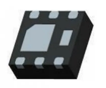


 工商网监
湘ICP备2023018690号
工商网监
湘ICP备2023018690号
